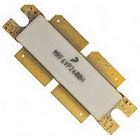
MRF6VP3450HR5 Freescale Semiconductor, MRF6VP3450HR5 Datasheet

MRF6VP3450HR5
Specifications of MRF6VP3450HR5
Available stocks
Related parts for MRF6VP3450HR5
MRF6VP3450HR5 Summary of contents
Page 1
... Freescale Semiconductor, Inc., 2008--2010. All rights reserved. RF Device Data Freescale Semiconductor = 50 Volts 1400 mA Volts 1400 mA Operation DD MRF6VP3450HR6 MRF6VP3450HR5 MRF6VP3450HSR6 MRF6VP3450HSR5 Document Number: MRF6VP3450H Rev. 4, 4/2010 MRF6VP3450HR6 MRF6VP3450HR5 MRF6VP3450HSR6 MRF6VP3450HSR5 860 MHz, 450 LATERAL N- -CHANNEL BROADBAND RF POWER MOSFETs CASE 375D- -05, STYLE 1 NI- -1230 ...
Page 2
... MTTF calculators by product. 2. Refer to AN1955, Thermal Measurement Methodology of RF Power Amplifiers http://www.freescale.com/rf. Select Documentation/Application Notes -- AN1955. 3. Each side of device measured separately. 4. Measurement made with device in push--pull configuration. 5. Part internally input matched. MRF6VP3450HR6 MRF6VP3450HR5 MRF6VP3450HSR6 MRF6VP3450HSR5 2 = 25°C unless otherwise noted) A Symbol I ...
Page 3
... Intermodulation Distortion Input Return Loss RF Device Data Freescale Semiconductor = 25°C unless otherwise noted) (continued) A Symbol G ps η D IRL P1dB G ps η D IM3 IRL MRF6VP3450HR6 MRF6VP3450HR5 MRF6VP3450HSR6 MRF6VP3450HSR5 Min Typ Max = 50 Vdc 1200 mA 520 out — 20.5 — — 50 — — --3 — ...
Page 4
... Microstrip Z10, Z11 0.150″ x 0.394″ Microstrip Z12, Z13 0.359″ x 0.394″ Microstrip Z14, Z15 0.308″ x 0.394″ Microstrip Figure 2. MRF6VP3450HR6(HSR6) Test Circuit Schematic MRF6VP3450HR6 MRF6VP3450HR5 MRF6VP3450HSR6 MRF6VP3450HSR5 4 Z19 C36 C38 R3 Z18 Z12 Z14 ...
Page 5
... ATC100B120GT500XT ATC100B6R8BT500XT ATC100B100GT500XT ATC800B6R8BT500XT ATC800B100J500XT ATC800B4R7J500XT ATC800B3R9J500XT ATC100B331GT500XT UUD1V220MCL1GS EEVFK2A221M C5750X5R1H106MT ATC200B393KT50XT ATC100B102JT500XT ATC100B471JT500XT HMK432BJ225KM--T C3225X7R1H225MT CRCW120610R0FKEA CRCW12061R50FKEA MRF6VP3450HR6 MRF6VP3450HR5 MRF6VP3450HSR6 MRF6VP3450HSR5 Part Number Manufacturer Fair--Rite ATC ATC ATC ATC ATC ATC ATC ATC Nichicon Panasonic TDK ATC ATC ATC ...
Page 6
... C24 C36 C34 C38 C44 C45 C35 B2 C25 C37 C39 R2 Figure 3. MRF6VP3450HR6(HSR6) Test Circuit Component Layout — Top Figure 3a. MRF6VP3450HR6(HSR6) Test Circuit Component Layout — Bottom MRF6VP3450HR6 MRF6VP3450HR5 MRF6VP3450HSR6 MRF6VP3450HSR5 6 MRF6VP3450H R3 C22 C13 C11 C12 C14 C23 R4 Rev. 4 C28 C26 C40 C7 ...
Page 7
... Pulse Width = 50 μsec, Duty Cycle = 2. --30_C 85_C 19 18 500 600 700 10 Figure 9. Pulsed Power Gain and Drain Efficiency MRF6VP3450HR6 MRF6VP3450HR5 MRF6VP3450HSR6 MRF6VP3450HSR5 T = 150_C 175_C 200_C 25_C DRAIN--SOURCE VOLTAGE (VOLTS) DS Figure 5. DC Safe Operating Area Ideal P3dB = 57.85 dBm (610 Vdc, I ...
Page 8
... Vdc 859.9 MHz 860 MHz DD 21.2 Two--Tone Measurements, 100 kHz Tone Spacing OUTPUT POWER (WATTS) PEP out Figure 12. Two- -Tone Power Gain versus Output Power MRF6VP3450HR6 MRF6VP3450HR5 MRF6VP3450HSR6 MRF6VP3450HSR5 8 -- Vdc 450 W (PEP out Two--Tone Measurements --20 3rd Order --30 --40 5th Order ...
Page 9
... P , OUTPUT POWER (WATTS) AVG. out Figure 18. Single- -Carrier DVB- -T OFDM ACPR Power Gain and Drain Efficiency versus Output Power MRF6VP3450HR6 MRF6VP3450HR5 MRF6VP3450HSR6 MRF6VP3450HSR5 7.61 MHz 4 kHz BW 4 kHz BW ACPR Measured at 4 MHz Offset from Center Frequency 8K Mode DVB--T OFDM 64 QAM Data Carrier Modulation, 5 Symbols ...
Page 10
... MHz ACPR Figure 21. Single- -Carrier DVB- -T OFDM ACPR, Power Gain and Drain Efficiency versus Output Power — 470- -860 MHz MRF6VP3450HR6 MRF6VP3450HR5 MRF6VP3450HSR6 MRF6VP3450HSR5 860 MHz 665 MHz 860 MHz 470 MHz 665 MHz 470 MHz η Vdc 1200 mA ...
Page 11
... JUNCTION TEMPERATURE (°C) J This above graph displays calculated MTTF in hours when the device is operated Vdc Avg., and η DD out MTTF calculator available at http://www.freescale.com/rf. Select Software & Tools/Development Tools/Calculators to access MTTF calculators by product. Figure 23. MTTF versus Junction Temperature MRF6VP3450HR6 MRF6VP3450HR5 MRF6VP3450HSR6 MRF6VP3450HSR5 -- --4 --6 ...
Page 12
... MHz Input Matching Network Figure 24. Series Equivalent Source and Load Impedance MRF6VP3450HR6 MRF6VP3450HR5 MRF6VP3450HSR6 MRF6VP3450HSR5 Ω 860 MHz Z load f = 470 MHz Z source f = 470 MHz Vdc 1400 mA Avg out source load MHz Ω Ω 470 2.81 -- j1.88 5.52 + j2.34 650 6.46 + j1.21 7 ...
Page 13
... RF Device Data Freescale Semiconductor PACKAGE DIMENSIONS MRF6VP3450HR6 MRF6VP3450HR5 MRF6VP3450HSR6 MRF6VP3450HSR5 13 ...
Page 14
... MRF6VP3450HR6 MRF6VP3450HR5 MRF6VP3450HSR6 MRF6VP3450HSR5 14 RF Device Data Freescale Semiconductor ...
Page 15
... RF Device Data Freescale Semiconductor MRF6VP3450HR6 MRF6VP3450HR5 MRF6VP3450HSR6 MRF6VP3450HSR5 15 ...
Page 16
... MRF6VP3450HR6 MRF6VP3450HR5 MRF6VP3450HSR6 MRF6VP3450HSR5 16 RF Device Data Freescale Semiconductor ...
Page 17
... Fig. 2, Test Circuit Schematic, Z--list, corrected Z4, Z5 from 1.400″ x 0.590″ Microstrip to 1.400″ x 0.059″ Microstrip Device Data Freescale Semiconductor REVISION HISTORY Description copy to read ”Test circuit impedance as measured from drain to load ng 10:1 VSWR @ 50 Vdc, 850 MHz, 450 Watts CW symbol θJC MRF6VP3450HR6 MRF6VP3450HR5 MRF6VP3450HSR6 MRF6VP3450HSR5 copy to read ”Test circuit source copy to read ”Test circuit load 17 ...
Page 18
... For Literature Requests Only: Freescale Semiconductor Literature Distribution Center 1--800--441--2447 or +1--303--675--2140 Fax: +1--303--675--2150 LDCForFreescaleSemiconductor@hibbertgroup.com MRF6VP3450HR6 MRF6VP3450HR5 MRF6VP3450HSR6 MRF6VP3450HSR5 Document Number: MRF6VP3450H Rev. 4, 4/2010 18 Information in this document is provided solely to enable system and software implementers to use Freescale Semiconductor products. There are no express or implied copyright licenses granted hereunder to design or fabricate any integrated circuits or integrated circuits based on the information in this document ...


