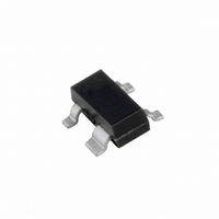
BF1100,215 NXP Semiconductors, BF1100,215 Datasheet

BF1100,215
Specifications of BF1100,215
BF1100 T/R
BF1100 T/R
Related parts for BF1100,215
BF1100,215 Summary of contents
Page 1
... IMPORTANT NOTICE Dear customer, As from October 1st, 2006 Philips Semiconductors has a new trade name - NXP Semiconductors, which will be used in future data sheets together with new contact details. In data sheets where the previous Philips references remain, please use the new links as shown below. ...
Page 2
... NXP Semiconductors Dual-gate MOS-FETs FEATURES Specially designed for use supply voltage Short channel transistor with high forward transfer admittance to input capacitance ratio Low noise gain controlled amplifier GHz Superior cross-modulation performance during AGC. APPLICATIONS VHF and UHF applications such as television tuners and professional communications equipment ...
Page 3
... NXP Semiconductors Dual-gate MOS-FETs LIMITING VALUES In accordance with the Absolute Maximum Rating System (IEC 134). SYMBOL PARAMETER V drain-source voltage DS I drain current D I gate 1 current G1 I gate 2 current G2 P total power dissipation tot BF1100 BF1100R T storage temperature stg T operating junction temperature ...
Page 4
... NXP Semiconductors Dual-gate MOS-FETs THERMAL CHARACTERISTICS SYMBOL R thermal resistance from junction to ambient th j-a BF1100 BF1100R R thermal resistance from junction to soldering point th j-s BF1100 BF1100R Notes 1. Device mounted on a printed-circuit board the temperature at the soldering point of the source lead. s STATIC CHARACTERISTICS unless otherwise specified. ...
Page 5
... NXP Semiconductors Dual-gate MOS-FETs DYNAMIC CHARACTERISTICS Common source amb SYMBOL PARAMETER y forward transfer admittance fs C input capacitance at gate 1 ig1-s C input capacitance at gate 2 ig2-s C drain-source capacitance os C reverse transfer capacitance MHz rs F noise figure 0 handbook, halfpage gain reduction (dB MHz Fig.5 Gain reduction as a function of the AGC voltage ...
Page 6
... NXP Semiconductors Dual-gate MOS-FETs 20 handbook, halfpage 1 (mA) 16 1 1 Fig.7 Output characteristics; typical values. 250 handbook, halfpage 200 150 100 Fig.9 Gate 1 current as a function of gate 1 voltage; typical values. MLD159 handbook, halfpage I D (mA ( Fig.8 Transfer characteristics; typical values. MLD161 ...
Page 7
... NXP Semiconductors Dual-gate MOS-FETs 16 handbook, halfpage I D (mA G2 Fig.11 Drain current as a function of gate 1 current; typical values. 12 handbook, halfpage I D (mA G2 180 k connected Fig.13 Drain current as a function of gate 1 voltage (= V ); typical values; see Fig.27. GG MLD163 handbook, halfpage MLD165 handbook, halfpage (V) GG ...
Page 8
... NXP Semiconductors Dual-gate MOS-FETs 50 handbook, halfpage 180 k (connected Fig.15 Gate 1 current as a function of gate 2 voltage; typical values. 16 handbook, halfpage I D (mA 180 k (connected Fig.17 Drain current as a function of the gate 2 voltage; typical values; see Fig.27. MLD167 handbook, halfpage ( 250 k (connected Fig.16 Gate 1 current as a function of gate 2 voltage; ...
Page 9
... NXP Semiconductors Dual-gate MOS-FETs 2 10 handbook, halfpage y is (mS mA amb Fig.19 Input admittance as a function of frequency; typical values (mS mA amb Fig.21 Forward transfer admittance and phase as a function of frequency; typical values. MLD172 (MHz mA Fig.20 Reverse transfer admittance and phase as MLD174 2 10 ...
Page 10
... NXP Semiconductors Dual-gate MOS-FETs 2 10 handbook, halfpage y is (mS mA amb Fig.23 Input admittance as a function of frequency; typical values (mS mA amb Fig.25 Forward transfer admittance and phase as a function of frequency; typical values. MLD176 (MHz mA Fig.24 Reverse transfer admittance and phase as MLD178 2 10 ...
Page 11
... NXP Semiconductors Dual-gate MOS-FETs handbook, full pagewidth R GEN For 180 For 250 AGC 4 DUT 4 Fig.27 Cross-modulation test set-up. Rev November 2007 Product specification BF1100; BF1100R 450 nH C4 4.7 nF MGC420 ...
Page 12
... NXP Semiconductors Dual-gate MOS-FETs Table 1 Scattering parameters MAGNITUDE ANGLE (MHz) (ratio) (deg) 50 0.986 3.6 100 0.983 7.4 200 0.974 14.7 300 0.960 21.8 400 0.953 28.7 500 0.933 35.4 600 0.915 42.0 700 0.895 47.9 800 0.880 53.5 900 0.864 59.6 1000 0 ...
Page 13
... NXP Semiconductors Dual-gate MOS-FETs PACKAGE OUTLINES handbook, full pagewidth 0.75 0. max 1.1 max Dimensions in mm. handbook, full pagewidth 0.40 0. max 1.1 max Dimensions in mm. 3.0 2.8 0.150 1.9 0.090 4 3 0.1 max o 10 max 0.88 0.48 max 0.1 1.7 TOP VIEW Fig ...
Page 14
... Right to make changes — NXP Semiconductors reserves the right to make changes to information published in this document, including without limitation specifications and product descriptions, at any time and without notice ...
Page 15
... NXP Semiconductors Revision history Revision history Document ID Release date BF1100_N_2 20071113 • Modifications: Fig. 1 and 2 on page 2; Figure note changed BF1100_1 19950425 Data sheet status Change notice Product data sheet - Product specification - Please be aware that important notices concerning this document and the product(s) described herein, have been included in section ‘ ...


