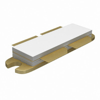
BLF6G22-180PN,112 NXP Semiconductors, BLF6G22-180PN,112 Datasheet

BLF6G22-180PN,112
Specifications of BLF6G22-180PN,112
BLF6G22-180PN
BLF6G22-180PN
Related parts for BLF6G22-180PN,112
BLF6G22-180PN,112 Summary of contents
Page 1
... BLF6G22-180PN Power LDMOS transistor Rev. 02 — 23 April 2008 1. Product profile 1.1 General description 180 W LDMOS power transistor for base station applications at frequencies from 2000 MHz to 2200 MHz. Table 1. RF performance at T Mode of operation 2-carrier W-CDMA [1] Test signal: 3GPP; test model 1; 64 DPCH; PAR = 7 0.01 % probability on CCDF per carrier; ...
Page 2
... RF power amplifiers for W-CDMA base stations and multicarrier applications in the 2000 MHz to 2200 MHz frequency range 2. Pinning information Table 2. Pin [1] Connected to flange. 3. Ordering information Table 3. Type number BLF6G22-180PN - 4. Limiting values Table 4. In accordance with the Absolute Maximum Rating System (IEC 60134). Symbol stg T case ...
Page 3
... Mode of operation: 1-carrier W-CDMA; PAR 7 0.01 % probability on CCDF; 3GPP test model PDPCH 1600 mA Symbol Parameter PAR O 7.1 Ruggedness in class-AB operation The BLF6G22-180PN is capable of withstanding a load mismatch corresponding to VSWR = through all phases under the following conditions 1600 mA BLF6G22-180PN_2 Product data sheet Characteristics Conditions ...
Page 4
... MHz One-tone CW power gain and drain efficiency as functions of load power; typical values 001aah633 50 D (%) IMD (dBc 200 300 P (W) L(PEP) = 2170 MHz; 1 Fig 3. Rev. 02 — 23 April 2008 BLF6G22-180PN Power LDMOS transistor 001aah632 60 D (%) 100 150 200 P ( IMD3 30 IMD5 IMD7 100 ...
Page 5
... Fig 5. 001aah637 35 D ACPR, (%) IMD3 30 (dBc (W) L(AV) = 2157.5 MHz; 1 Fig 7. Rev. 02 — 23 April 2008 BLF6G22-180PN Power LDMOS transistor 1600 mA 2162.5 MHz 2167.5 MHz; carrier spacing 5 MHz. 2 2-carrier W-CDMA adjacent channel power ratio as function of average load power; typical values 20 30 IMD3 ACPR ...
Page 6
... Fig 8. BLF6G22-180PN_2 Product data sheet See Table 9 for list of components. Test circuit for operation at 2110 MHz and 2170 MHz Rev. 02 — 23 April 2008 BLF6G22-180PN Power LDMOS transistor C10 C11 R2 C12 R3 C14 C15 C16 output 50 C13 001aah639 © NXP B.V. 2008. All rights reserved. ...
Page 7
... ATC multilayer ceramic chip capacitor ATC multilayer ceramic chip capacitor chip resistor chip resistor Rev. 02 — 23 April 2008 BLF6G22-180PN Power LDMOS transistor C10 C11 C13 C12 OUTPUT C14 C15 C16 TB BLF6G22-180PN 001aah640 = 3.5 and thickness = 0.76 mm. r Value Remarks [ 4.7 F 220 nF [ 220 100 nF [ [1] 0 ...
Page 8
... H 31.52 9.50 9.53 1.75 17.12 25.53 13.72 30.96 9.30 9.27 1.50 16.10 25.27 1.241 0.374 0.375 0.069 0.674 1.005 0.540 1.219 0.366 0.365 0.634 0.059 0.995 REFERENCES JEDEC EIAJ Rev. 02 — 23 April 2008 BLF6G22-180PN Power LDMOS transistor 3.73 3.30 2.31 41.28 10 ...
Page 9
... Power of the Dedicated Physical CHannel Radio Frequency Voltage Standing-Wave Ratio Wideband Code Division Multiple Access Data sheet status Product data sheet Preliminary data sheet Rev. 02 — 23 April 2008 BLF6G22-180PN Power LDMOS transistor Change notice Supersedes - BLF6G22-180PN_1 - - © NXP B.V. 2008. All rights reserved ...
Page 10
... Trademarks Notice: All referenced brands, product names, service names and trademarks are the property of their respective owners. http://www.nxp.com salesaddresses@nxp.com Rev. 02 — 23 April 2008 BLF6G22-180PN Power LDMOS transistor © NXP B.V. 2008. All rights reserved ...
Page 11
... Please be aware that important notices concerning this document and the product(s) described herein, have been included in section ‘Legal information’. © NXP B.V. 2008. For more information, please visit: http://www.nxp.com For sales office addresses, please send an email to: salesaddresses@nxp.com Document identifier: BLF6G22-180PN_2 All rights reserved. Date of release: 23 April 2008 ...


