MW6S010NR1 Freescale Semiconductor, MW6S010NR1 Datasheet
MW6S010NR1
Specifications of MW6S010NR1
MW6S010NR1TR
Available stocks


Related parts for MW6S010NR1


MW6S010NR1 Summary of contents
Page 1
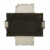
... LATERAL N - CHANNEL BROADBAND RF POWER MOSFETs CASE 1265 - 09, STYLE 270 - 2 PLASTIC MW6S010NR1 CASE 1265A - 03, STYLE 270 - 2 GULL PLASTIC MW6S010GNR1 Symbol Value Unit V - 0.5, +68 Vdc DSS V - 0.5, +12 Vdc +150 °C stg T 150 ° 225 °C J (2,3) Symbol Value Unit R °C/W θJC 2.85 MW6S010NR1 MW6S010GNR1 1 ...
Page 2
... Drain Efficiency Intermodulation Distortion Input Return Loss Typical Performances (In Freescale 450 MHz Demo Board, 50 οhm system) V Two - Tone Test, 100 kHz Tone Spacing Power Gain Drain Efficiency Intermodulation Distortion Input Return Loss MW6S010NR1 MW6S010GNR1 2 Rating 3 = 25°C unless otherwise noted) A Symbol I DSS ...
Page 3
... Microstrip Z3 0.213″ x 0.500″ Microstrip Z4 0.313″ x 1.503″ Microstrip Figure 1. MW6S010NR1(GNR1) Test Circuit Schematic — 900 MHz Table 6. MW6S010NR1(GNR1) Test Circuit Component Designations and Values — 900 MHz Part B1 C1, C6, C11, C20 C2, C18, C19 C3, C16 ...
Page 4
... MW6S010N Figure 2. MW6S010NR1(GNR1) Test Circuit Component Layout — 900 MHz MW6S010NR1 MW6S010GNR1 4 C7 C10 C11 C18 C16 C15 C19 C13 C12 C20 C17 C14 RF Device Data Freescale Semiconductor ...
Page 5
... Order DQ 5th Order 7th Order OUTPUT POWER (WATTS) AVG. out versus Output Power P3dB = 43.14 dBm (20. Vdc 125 Pulsed CW, 8 μsec(on), 1 msec(off 945 MHz INPUT POWER (dBm) in Figure 7. Pulse CW Output Power versus Input Power MW6S010NR1 MW6S010GNR1 100 Ideal Actual 29 5 ...
Page 6
... OUTPUT POWER (WATTS) CW out Figure 10. Power Gain versus Output Power MW6S010NR1 MW6S010GNR1 6 TYPICAL CHARACTERISTICS — 900 MHz Vdc 125 945 MHz G ps η D ACPR OUTPUT POWER (WATTS) AVG. out Figure 8. Single - Carrier CDMA ACPR, Power Gain and Power Added Efficiency versus Output Power − ...
Page 7
... T , JUNCTION TEMPERATURE (°C) J This above graph displays calculated MTTF in hours when the device = 10 W PEP, and η is operated Vdc out MTTF calculator available at http://www.freescale.com/rf. Select Software & Tools/Development Tools/Calculators to access MTTF calculators by product. 210 230 250 = 32%. D MW6S010NR1 MW6S010GNR1 7 ...
Page 8
... MHz Z source f = 800 MHz Figure 13. Series Equivalent Source and Load Impedance — 900 MHz MW6S010NR1 MW6S010GNR1 Ω 980 MHz Z load f = 800 MHz Vdc 125 mA PEP DD DQ out source load MHz Ω Ω 800 3.1 + j1.9 10.1 + j2.3 2.8 + j1.7 820 8 ...
Page 9
... Microstrip Z3 0.225″ x 0.080″ Microstrip Z4, Z7 0.440″ x 0.080″ Microstrip Figure 14. MW6S010NR1(GNR1) Test Circuit Schematic — 450 MHz Table 7. MW6S010NR1(GNR1) Test Circuit Component Designations and Values — 450 MHz Part B1 C2, C15 C3, C14 C4, C9, C10, C13 ...
Page 10
... MW6S010N 450 MHz Figure 15. MW6S010NR1(GNR1) Test Circuit Component Layout — 450 MHz MW6S010NR1 MW6S010GNR1 C14 C15 C13 C12 C10 C11 RF Device Data Freescale Semiconductor ...
Page 11
... Watts Avg. out = 150 mA, DQ ACPR ALT1 ALT2 OUTPUT POWER (WATTS) AVG. out and ALT2 versus Output Power MW6S010NR1 MW6S010GNR1 −10 −20 −30 −40 −50 −60 −70 −80 11 ...
Page 12
... MHz Figure 20. Series Equivalent Source and Load Impedance — 450 MHz MW6S010NR1 MW6S010GNR1 Ω 500 MHz Z source f = 500 MHz Z load f = 400 MHz Vdc 150 mA PEP DD DQ out source load MHz Ω Ω 400 9.0 + j3.8 15.0 + j1.4 8.8 + j5.4 420 14 ...
Page 13
... RF Device Data Freescale Semiconductor PACKAGE DIMENSIONS MW6S010NR1 MW6S010GNR1 13 ...
Page 14
... MW6S010NR1 MW6S010GNR1 14 RF Device Data Freescale Semiconductor ...
Page 15
... RF Device Data Freescale Semiconductor MW6S010NR1 MW6S010GNR1 15 ...
Page 16
... MW6S010NR1 MW6S010GNR1 16 RF Device Data Freescale Semiconductor ...
Page 17
... RF Device Data Freescale Semiconductor MW6S010NR1 MW6S010GNR1 17 ...
Page 18
... MW6S010NR1 MW6S010GNR1 18 RF Device Data Freescale Semiconductor ...
Page 19
... Added Electromigration MTTF Calculator and RF High Power Model availability to Product Software Device Data Freescale Semiconductor REVISION HISTORY Description the RF test condition voltage callout for test condition to indicate AC stimulus on the V iss and added “Measured in Functional GS(Q) connection versus the V connection and listed MW6S010NR1 MW6S010GNR1 19 ...
Page 20
... For Literature Requests Only: Freescale Semiconductor Literature Distribution Center 1 - 800 - 441 - 2447 303 - 675 - 2140 Fax 303 - 675 - 2150 LDCForFreescaleSemiconductor@hibbertgroup.com MW6S010NR1 MW6S010GNR1 Document Number: MW6S010N Rev. 5, 6/2009 20 Information in this document is provided solely to enable system and software implementers to use Freescale Semiconductor products. There are no express or implied copyright licenses granted hereunder to design or fabricate any integrated circuits or integrated circuits based on the information in this document ...