MRF5S9100NBR1 Freescale Semiconductor, MRF5S9100NBR1 Datasheet
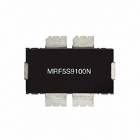
MOSFET N-CH 100W 26V TO-272-4

MRF5S9100NBR1

Manufacturer Part Number
MRF5S9100NBR1
Description
MOSFET N-CH 100W 26V TO-272-4
Manufacturer
Freescale Semiconductor
Datasheet

Specifications of MRF5S9100NBR1

Transistor Type
N-Channel
Frequency
880MHz
Gain
19.5dB
Voltage - Rated
68V
Current Rating
10µA
Current - Test
950mA
Voltage - Test
26V
Power - Output
20W
Package / Case
TO-272-4
Lead Free Status / RoHS Status
Lead free / RoHS Compliant
Noise Figure
-
Other names
MRF5S9100NBR1TR

Available stocks

Company
Part Number
Manufacturer
Quantity
Price
Part Number:
MRF5S9100NBR1
Manufacturer:
FREESCALE
Quantity:
1 400
Part Number:
MRF5S9100NBR1
Manufacturer:
FREESCALE
Quantity:
20 000
© Freescale Semiconductor, Inc., 2006. All rights reserved.
RF Device Data
Freescale Semiconductor
Technical Data
RF Power Field Effect Transistors
N - Channel Enhancement - Mode Lateral MOSFETs
frequencies up to 1000 MHz. The high gain and broadband performance of
these devices make them ideal for large - signal, common - source amplifier
applications in 26 volt base station equipment.
• Typical Single - Carrier N - CDMA Performance @ 880 MHz, V
• Capable of Handling 10:1 VSWR, @ 26 Vdc, 880 MHz, 100 Watts CW
• Characterized with Series Equivalent Large - Signal Impedance Parameters
• Internally Matched for Ease of Use
• Qualified Up to a Maximum of 32 V
• Integrated ESD Protection
• 200°C Capable Plastic Package
• In Tape and Reel. R1 Suffix = 500 Units per 44 mm, 13 inch Reel.
Table 1. Maximum Ratings
Table 2. Thermal Characteristics
Replaced by MRF5S9100NR1/NBR1. There are no form, fit or function changes with
this part replacement. N suffix added to part number to indicate transition to lead - free
terminations.
Drain- Source Voltage
Gate - Source Voltage
Total Device Dissipation @ T
Storage Temperature Range
Operating Junction Temperature
Thermal Resistance, Junction to Case
Designed for broadband commercial and industrial applications with
1. MTTF calculator available at http://www.freescale.com/rf. Select Tools/Software/Application Software/Calculators to access
2. Refer to AN1955, Thermal Measurement Methodology of RF Power Amplifiers. Go to http://www.freescale.com/rf.
I
Traffic Codes 8 Through 13) Channel Bandwidth = 1.2288 MHz. PAR =
9.8 dB @ 0.01% Probability on CCDF.
Output Power
DQ
Derate above 25°C
Case Temperature 80°C, 20 W CW
NOTE - CAUTION - MOS devices are susceptible to damage from electrostatic charge. Reasonable precautions in handling and
packaging MOS devices should be observed.
Power Gain — 19.5 dB
Drain Efficiency — 28%
ACPR @ 750 kHz Offset — - 46.8 dBc @ 30 kHz Bandwidth
the MTTF calculators by product.
Select Documentation/Application Notes - AN1955.
= 950 mA, P
out
= 20 Watts Avg., IS - 95 CDMA (Pilot, Sync, Paging,
C
= 25°C
Characteristic
Rating
DD
Operation
DD
= 26 Volts,
Symbol
Symbol
V
R
V
T
P
DSS
T
θJC
GS
stg
D
J
CASE 1486 - 03, STYLE 1
Document Number: MRF5S9100
MRF5S9100MBR1
MRF5S9100MR1 MRF5S9100MBR1
MRF5S9100MR1
880 MHz, 20 W AVG., 26 V
MRF5S9100MR1
LATERAL N - CHANNEL
TO - 270 WB - 4
RF POWER MOSFETs
PLASTIC
SINGLE N - CDMA
- 65 to +150
Value
- 0.5, +68
- 0.5, + 15
CASE 1484 - 04, STYLE 1
Value
1.92
0.52
336
200
MRF5S9100MBR1
(1,2)
TO - 272 WB - 4
PLASTIC
Rev. 4, 5/2006
W/°C
°C/W
Unit
Unit
Vdc
Vdc
°C
°C
W
1

Related parts for MRF5S9100NBR1

MRF5S9100NBR1 Summary of contents

Page 1

... Refer to AN1955, Thermal Measurement Methodology of RF Power Amplifiers http://www.freescale.com/rf. Select Documentation/Application Notes - AN1955. NOTE - CAUTION - MOS devices are susceptible to damage from electrostatic charge. Reasonable precautions in handling and packaging MOS devices should be observed. © Freescale Semiconductor, Inc., 2006. All rights reserved. RF Device Data Freescale Semiconductor = 26 Volts, ...

Page 2

... Vdc — 3.7 — Vdc — 0.21 0.3 Vdc — 7 — S — 70 — pF — 2.2 — Avg CDMA 880 MHz, out 18 19.5 — — % — dBc — Device Data Freescale Semiconductor ...

Page 3

... Chip Capacitors C9, C10 5.1 pF Chip Capacitors C13 470 mF Electrolytic Capacitor C14, C15 22 mF Tantalum Capacitors C16, C17, C19 0.56 mF Chip Capacitors C20, C21 47 mF Tantalum Capacitors C22 100 mF Electrolytic Capacitor L1 7.15 nH Inductor Inductor RF Device Data Freescale Semiconductor C18 Z10 DUT Z10 Z12 ...

Page 4

... Freescale has begun the transition of marking Printed Circuit Boards (PCBs) with the Freescale Semiconductor signature/logo. PCBs may have either Motorola or Freescale markings during the transition period. These changes will have no impact on form, fit or function of the current product. Figure 2. MRF5S9100MR1(MBR1) Test Circuit Component Layout ...

Page 5

... Vdc 880 MHz 880.1 MHz DD Two −Tone Measurements, 100 kHz Tone Spacing 16 0 OUTPUT POWER (WATTS) PEP out Figure 5. Two - Tone Power Gain versus Output Power RF Device Data Freescale Semiconductor TYPICAL CHARACTERISTICS G ps η Vdc (Avg.), I = 950 mA DD out DQ N−CDMA IS−95 (Pilot, Sync, Paging, Traffic ...

Page 6

... Pulsed CW, 8 μsec(on), 1 msec(off) Center Frequency = 880 MHz INPUT POWER (dBm) in Input Power −30 −35 −40 −45 −50 −55 −60 −65 −70 −75 −80 100 120 140 160 180 200 T , JUNCTION TEMPERATURE (° for MTTF in a particular application Device Data Freescale Semiconductor 38 220 ...

Page 7

... MHz f = 865 MHz Figure 12. Series Equivalent Source and Load Impedance RF Device Data Freescale Semiconductor Z load f = 865 MHz f = 895 MHz Z source = 5 Ω Vdc 950 mA Avg out source load MHz Ω Ω 865 3.0 - j1.8 1.4 - j0.7 880 2.8 - j1.9 1.5 - j0.6 895 2 ...

Page 8

... E5 .346 .350 8.79 8.89 F .025 BSC 0.64 BSC b1 .164 .170 4.17 4.32 c1 .007 .011 0.18 0.28 e .106 BSC 2.69 BSC aaa .004 0.10 STYLE 1: PIN 1. DRAIN 2. DRAIN 3. GATE 4. GATE 5. SOURCE RF Device Data Freescale Semiconductor ...

Page 9

... RF Device Data Freescale Semiconductor MRF5S9100MR1 MRF5S9100MBR1 9 ...

Page 10

... MRF5S9100MR1 MRF5S9100MBR1 10 RF Device Data Freescale Semiconductor ...

Page 11

... RF Device Data Freescale Semiconductor MRF5S9100MR1 MRF5S9100MBR1 11 ...

Page 12

... Freescale Semiconductor product could create a situation where personal injury or death may occur. Should Buyer ...

Related keywords