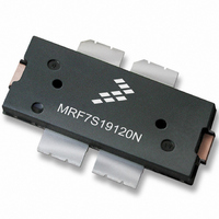
MRF7S19120NR1 Freescale Semiconductor, MRF7S19120NR1 Datasheet

MRF7S19120NR1
Specifications of MRF7S19120NR1
Related parts for MRF7S19120NR1
MRF7S19120NR1 Summary of contents
Page 1
... MHz AVG Symbol V DSS stg Symbol R θJC Rev. 2, 12/2009 SINGLE W-CDMA LATERAL N-CHANNEL RF POWER MOSFET CASE 1730-02 TO-270 WBL-4 PLASTIC Value Unit -0.5, +65 Vdc -6.0, +10 Vdc 32, +0 Vdc °C -65 to +150 °C 150 °C 225 (2,3) Value Unit °C/W 0.43 0.51 MRF7S19120NR1 1 ...
Page 2
... MHz, Single-Carrier W-CDMA, IQ Magnitude Clipping, Input Signal PAR = 7 0.01% Probability on CCDF. ACPR measured in 3.84 MHz Channel Bandwidth @ ±5 MHz Offset. Power Gain Drain Efficiency Output Peak-to-Average Ratio @ 0.01% Probability on CCDF Adjacent Channel Power Ratio Input Return Loss 1. Part internally matched both on input and output. MRF7S19120NR1 2 Rating 3 = 25°C unless otherwise noted) A Symbol I ...
Page 3
... W CW, out ΔG ΔP1dB Min Typ Max = 1200 mA, 1930-1990 MHz Bandwidth — 20 — — 0.495 — — 0.914 — — 1.98 — — 33.9 — — 0.016 — — 0.009 — MRF7S19120NR1 Unit MHz dB ° ns ° dB/°C dBm/°C 3 ...
Page 4
... Z5 1.000″ x 0.125″ Microstrip Z6 1.000″ x 0.090″ Microstrip Z7 0.880″ x 0.111″ Microstrip Figure 1. MRF7S19120NR1 Test Circuit Schematic Table 6. MRF7S19120NR1 Test Circuit Component Designations and Values Part 10 μ Tantalum Capacitor C1 0.01 μF Chip Capacitor C2 C3, C4, C8, C9 5.1 pF Chip Capacitors 10 μ ...
Page 5
... MRF7S19120N Rev. 3 Figure 2. MRF7S19120NR1 Test Circuit Component Layout RF Device Data Freescale Semiconductor C10 C11 MRF7S19120NR1 5 ...
Page 6
... Vdc 1955 MHz 1965 MHz DD Two-Tone Measurements, 10 MHz Tone Spacing OUTPUT POWER (WATTS) PEP out Figure 5. Two-T one Power Gain versus Output Power MRF7S19120NR1 6 TYPICAL CHARACTERISTICS G ps η Vdc (Avg.), I = 1200 mA DD out DQ Single-Carrier W-CDMA, 3.84 MHz Channel Bandwidth Input Signal PAR = 7 ...
Page 7
... Vdc 120 W (PEP 1200 mA out DQ IM3-U IM3-L IM5-U IM5-L IM7-U IM7-L 10 TWO-T ONE SPACING (MHz) versus Tone Spacing 50 Ideal Actual -30 _C 25_C G ps 25_C 85_C 85_C Vdc 1200 1960 MHz 10 100 P , OUTPUT POWER (WATTS) CW out versus CW Output Power MRF7S19120NR1 100 300 7 ...
Page 8
... Input Signal 0.1 0.01 W-CDMA. ACPR Measured in 3.84 MHz Channel Bandwidth @ ±5 MHz Offset. 0.001 Input Signal PAR = 7 0.01% Probability on CCDF 0.0001 PEAK-T O-A VERAGE (dB) Figure 14. CCDF W-CDMA IQ Magnitude Clipping, Single-Carrier Test Signal MRF7S19120NR1 8 TYPICAL CHARACTERISTICS 1200 1960 MHz 160 200 ...
Page 9
... Z = Test circuit impedance as measured from source gate to ground Test circuit impedance as measured from load drain to ground. Input Device Under Matching Test Network Z Z source load = 5 Ω Output Matching Network MRF7S19120NR1 9 ...
Page 10
... MRF7S19120NR1 10 PACKAGE DIMENSIONS RF Device Data Freescale Semiconductor ...
Page 11
... RF Device Data Freescale Semiconductor MRF7S19120NR1 11 ...
Page 12
... MRF7S19120NR1 12 RF Device Data Freescale Semiconductor ...
Page 13
... Added AN1907, Solder Reflow Attach Method for High Power RF Devices in Plastic Packages and AN3789, Clamping of High Power RF Transistors and RFICs in Over-Molded Plastic Packages to Product Documentation, Application Notes • Added Electromigration MTTF Calculator availability to Product Software Device Data Freescale Semiconductor REVISION HISTORY Description impedance source MRF7S19120NR1 13 ...
Page 14
... For Literature Requests Only: Freescale Semiconductor Literature Distribution Center 1-800-441-2447 or +1-303-675-2140 Fax: +1-303-675-2150 LDCForFreescaleSemiconductor@hibbertgroup.com MRF7S19120NR1 Document Number: MRF7S19120N Rev. 2, 12/2009 14 Information in this document is provided solely to enable system and software implementers to use Freescale Semiconductor products. There are no express or implied copyright licenses granted hereunder to design or fabricate any integrated circuits or integrated circuits based on the information in this document ...


