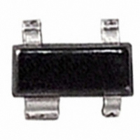
BF 1005S E6433 Infineon Technologies, BF 1005S E6433 Datasheet

BF 1005S E6433
Specifications of BF 1005S E6433
SP000010952
Related parts for BF 1005S E6433
BF 1005S E6433 Summary of contents
Page 1
Silicon N-Channel MOSFET Tetrode For low noise, high gain controlled input stages GHz Operating voltage 5 V Integrated biasing network Pb-free (RoHS compliant) package Qualified according AEC Q101 G2 AGC G1 RF Input GND ESD (Electrostatic discharge) ...
Page 2
Thermal Resistance Parameter 1) Channel - soldering point Electrical Characteristics at T Parameter DC Characteristics Drain-source breakdown voltage I = 650 µ G1S G2S Gate1-source breakdown voltage + mA ...
Page 3
Electrical Characteristics at T Parameter AC Characteristics (verified by random sampling) Forward transconductance 4 G2S Gate1 input capacitance MHz DS G2S ...
Page 4
Total power dissipation P BF1005S, BF1005SR 220 mW 180 160 140 120 100 Drain current G2S ...
Page 5
Forward transfer admittance | G2S 0.5 1 1.5 2 2.5 Output capacitance C dss f = 200MHz 1.5 1 0.5 ...
Page 6
Package Outline Foot Print Marking Layout (Example) Standard Packing Reel ø180 mm = 3.000 Pieces/Reel Reel ø330 mm = 10.000 Pieces/Reel Package SOT143 2.9 ±0 0.2 +0.1 0.8 -0.05 +0.1 0.4 -0.05 0.25 B ...
Page 7
Package Outline Foot Print Marking Layout (Example) Standard Packing Reel ø180 mm = 3.000 Pieces/Reel Reel ø330 mm = 10.000 Pieces/Reel Package SOT143R 2.9 ±0 0.2 +0.1 0.8 -0.05 +0.1 0.4 -0.05 1.7 0.2 ...
Page 8
... For information on the types in question please contact your nearest Infineon Technologies Office. Infineon Technologies Components may only be used in life-support devices or systems with the express written approval of Infineon Technologies failure of such components can reasonably be expected to cause the failure of that life-support device or system affect the safety or effectiveness of that device or system ...


