BFP450E6327 Infineon Technologies, BFP450E6327 Datasheet
BFP450E6327
Specifications of BFP450E6327
BFP450E6327XT
BFP450INTR
BFP450XTINTR
BFP450XTINTR
SP000011039
Available stocks


Related parts for BFP450E6327

BFP450E6327 Summary of contents
Page 1
High Linearity Low Noise Si NPN RF Transistor Revision 1.0, 2010-10- & ...
Page 2
... Infineon Technologies Office. Infineon Technologies components may be used in life-support devices or systems only with the express written approval of Infineon Technologies failure of such components can reasonably be expected to cause the failure of that life-support device or system or to affect the safety or effectiveness of that device or system. Life support devices or systems are intended to be implanted in the human body or to support and/or maintain and sustain and/or protect human life ...
Page 3
... Pulse load curves removed characteristic curves updated. Trademarks of Infineon Technologies AG AURIX™, BlueMoon™, COMNEON™, C166™, CROSSAVE™, CanPAK™, CIPOS™, CoolMOS™, CoolSET™, CORECONTROL™, DAVE™, EasyPIM™, EconoBRIDGE™, EconoDUAL™, EconoPACK™, EconoPIM™, EiceDRIVER™ ...
Page 4
Table of Contents Table of Contents . . . . . . . . . . . . . . . . . . . . . . . . . . . . . . . . . . ...
Page 5
List of Figures Figure 1 Total Power Dissipation Figure 2 BFP450 Testing Circuit ...
Page 6
List of Tables Table 1 Maximum Ratings . . . . . . . . . . . . . . . . . . . . . . . . . . . . . . . . . ...
Page 7
High Linearity Low Noise Si NPN RF Transistor 1 Features • Highly linear low noise driver amplifier for all RF frontends up to 2.5 GHz OP • Output compression point 1.9 GHz, 50 Ω system ...
Page 8
Maximum Ratings Table 1 Maximum Ratings Parameter Collector emitter voltage Collector emitter voltage Collector base voltage Emitter base voltage Collector current Base current 1) Total power dissipation Junction temperature Storage temperature the soldering point temperature. T ...
Page 9
Thermal Characteristics Table 2 Thermal Resistance Parameter Symbol 1) R Junction - soldering point thJS 1)For calculation of R please refer to Application Note Thermal Resistance AN077 thJA 600 600 500 500 400 400 300 300 200 200 100 ...
Page 10
Electrical Characteristics 4.1 DC Characteristics Table 3 DC Characteristics at Parameter Collector emitter breakdown voltage Collector emitter leakage current Collector base leakage current Emitter base leakage current DC current gain 4.2 General AC Characteristics Table 4 General AC Characteristics ...
Page 11
Frequency Dependent AC Characteristics Measurement setup is a test fixture with Bias T’ Ω system, VB Bias-T IN Figure 2 BFP450 Testing Circuit Table 5 AC Characteristics, Parameter Maximum power gain High linearity operation point Class ...
Page 12
Table 6 AC Characteristics, Parameter Maximum power gain High linearity operation point Class A operation point Transducer gain High linearity operation point Class A operation point Minimum noise figure Minimum noise figure Associated gain Linearity 1 dB gain compression point ...
Page 13
Table 8 AC Characteristics, Parameter Maximum power gain High linearity operation point Class A operation point Transducer gain High linearity operation point Class A operation point Minimum noise figure Minimum noise figure Associated gain Linearity 1 dB gain compression point ...
Page 14
Table 10 AC Characteristics, Parameter Maximum power gain High linearity operation point Class A operation point Transducer gain High linearity operation point Class A operation point Minimum noise figure Minimum noise figure Associated gain Linearity 1 dB gain compression point ...
Page 15
Characteristic DC Diagrams 160 140 120 100 Figure 3 Collector Current vs. Collector Emitter Voltage 120 110 100 0.1 h Figure 4 DC Current Gain Data Sheet 1 ...
Page 16
Figure 5 Collector Current vs. Base Emitter Voltage 10 1 0.1 0.01 0.001 0.0001 0.6 Figure 6 Base Current vs. Base Emitter Forward Voltage Data Sheet 0.65 0.7 0. ...
Page 17
Figure 7 Base Current vs. Base Emitter Reverse Voltage Data Sheet 0.4 0 Electrical Characteristics 1.2 1.4 1.6 1 ...
Page 18
Characteristic AC Diagrams Figure 8 Transition Frequency Figure 9 3rd Order Intercept Point Data Sheet 100 I ...
Page 19
Figure 10 Collector Base Capacitance 0 Figure 11 Gain , , I ma ...
Page 20
Figure 12 Maximum Power Gain 0.5 Figure 13 Maximum Power Gain ...
Page 21
S Figure 14 Input Matching 11 0.1 0 −0.1 Figure 15 Source Impedance for Minimum Noise Figure Data Sheet 0 0.4 4 0.3 3 0 GHz ...
Page 22
S Figure 16 Output Matching 3 2.5 2 1 Figure 17 Noise Figure min Data Sheet 0 ...
Page 23
NF Figure 18 Noise Figure min 4.5 4 3.5 3 2.5 2 1 Figure 19 Noise Figure 50 Data Sheet [mA ...
Page 24
Figure 20 Comparison Noise Figure Note: The curves shown in this chapter have been generated using typical devices but shall not be considered as a guarantee that all devices have ...
Page 25
Simulation Data For the SPICE Gummel Poon (GP) model as well as for the S-parameters (including noise parameters) please refer to our internet website: www.infineon.com/rf.models. Please consult our website and download the latest versions before actually starting your design. ...
Page 26
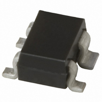
Package Information SOT343 Figure 21 Package Outline Figure 22 Package Foot Print Figure 23 Marking Description (Marking BFP450: ANs) Figure 24 Tape Dimensions Data Sheet 2 ±0.2 0.1 MAX. 1 +0.1 0.3 -0.05 ...
Page 27
... Published by Infineon Technologies AG ...