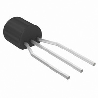
2N5060RLRMG ON Semiconductor, 2N5060RLRMG Datasheet - Page 2

2N5060RLRMG
Manufacturer Part Number
2N5060RLRMG
Description
THYRISTOR SCR 0.8A 30V TO-92
Manufacturer
ON Semiconductor
Type
SCRr
Datasheet
1.2N5064RLRAG.pdf
(7 pages)
Specifications of 2N5060RLRMG
Scr Type
Sensitive Gate
Voltage - Off State
30V
Voltage - Gate Trigger (vgt) (max)
800mV
Voltage - On State (vtm) (max)
1.7V
Current - On State (it (av)) (max)
510mA
Current - On State (it (rms)) (max)
800mA
Current - Gate Trigger (igt) (max)
200µA
Current - Hold (ih) (max)
5mA
Current - Off State (max)
10µA
Current - Non Rep. Surge 50, 60hz (itsm)
10A @ 60Hz
Operating Temperature
-40°C ~ 110°C
Mounting Type
Through Hole
Package / Case
TO-92-3 (Standard Body), TO-226
Current - On State (it (rms) (max)
800mA
Repetitive Peak Off-state Volt
30V
Off-state Voltage
30V
Average On-state Current
510mA
Hold Current
5mA
Gate Trigger Current (max)
200uA
Gate Trigger Voltage (max)
800mV
Peak Reverse Gate Voltage
5V
Package Type
TO-92
Peak Repeat Off Current
10uA
Peak Surge On-state Current (max)
10A
On State Voltage(max)
1.7@1.2AV
Mounting
Through Hole
Pin Count
3
Operating Temp Range
-40C to 110C
Operating Temperature Classification
Industrial
Lead Free Status / RoHS Status
Lead free / RoHS Compliant
Other names
2N5060RLRMG
2N5060RLRMGOSTB
2N5060RLRMGOSTB
Stresses exceeding Maximum Ratings may damage the device. Maximum Ratings are stress ratings only. Functional operation above the
Recommended Operating Conditions is not implied. Extended exposure to stresses above the Recommended Operating Conditions may affect
device reliability.
1. V
2. This measurement is made with the case mounted “flat side down” on a heatsink and held in position by means of a metal clamp over the
*Indicates JEDEC Registered Data.
MAXIMUM RATINGS
THERMAL CHARACTERISTICS
Peak Repetitive Off−State Voltage (Note 1)
On-State Current RMS (180° Conduction Angles; T
*Average On-State Current
*Peak Non-repetitive Surge Current,
Circuit Fusing Considerations (t = 8.3 ms)
*Average On-State Current
*Forward Peak Gate Power (Pulse Width v 1.0 msec; T
*Forward Average Gate Power (T
*Forward Peak Gate Current (Pulse Width v 1.0 msec; T
*Reverse Peak Gate Voltage (Pulse Width v 1.0 msec; T
*Operating Junction Temperature Range
*Storage Temperature Range
*Thermal Resistance, Junction−to−Case (Note 2)
Thermal Resistance, Junction−to−Ambient
voltage shall not be applied concurrent with negative potential on the anode. Blocking voltages shall not be tested with a constant current
source such that the voltage ratings of the devices are exceeded.
curved surface.
(T
50 to 60 Hz, R
(180° Conduction Angles)
(T
(T
T
(1/2 cycle, Sine Wave, 60 Hz)
(180° Conduction Angles)
(T
(T
DRM
A
J
C
C
C
C
= 25°C
= *40 to 110°C, Sine Wave,
= 67°C)
= 102°C)
= 67°C)
= 102°C)
and V
RRM
GK
for all types can be applied on a continuous basis. Ratings apply for zero or negative gate voltage; however, positive gate
= 1 kW)
(T
J
= 25°C unless otherwise noted)
A
= 25°C, t = 8.3 ms)
Characteristic
2N5060
2N5061
2N5062
2N5064
Rating
C
= 80°C)
A
A
http://onsemi.com
A
= 25°C)
= 25°C)
= 25°C)
2
Symbol
Symbol
I
V
P
V
T(RMS)
V
I
I
R
I
R
P
T(AV)
T(AV)
I
T
DRM,
TSM
G(AV)
RRM
RGM
I
GM
T
qJC
qJA
GM
stg
2
J
t
−40 to +150
−40 to +110
Value
0.255
0.255
0.51
0.51
0.01
Max
100
200
200
0.8
0.4
0.1
1.0
5.0
30
60
10
75
°C/W
°C/W
Unit
Unit
A
°C
°C
W
W
V
A
A
A
A
A
V
2
s


