MAT02EH Analog Devices Inc, MAT02EH Datasheet
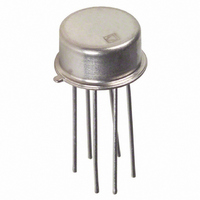
IC TX MATCHED MONO DUAL LN TO-78

MAT02EH

Manufacturer Part Number
MAT02EH
Description
IC TX MATCHED MONO DUAL LN TO-78
Manufacturer
Analog Devices Inc
Datasheet

Specifications of MAT02EH

Rohs Status
RoHS non-compliant
Transistor Type
2 NPN (Dual)
Current - Collector (ic) (max)
20mA
Voltage - Collector Emitter Breakdown (max)
40V
Vce Saturation (max) @ Ib, Ic
100mV @ 100µA, 1mA
Current - Collector Cutoff (max)
3nA
Power - Max
1.8W
Frequency - Transition
200MHz
Mounting Type
Through Hole
Package / Case
TO-78-6 Metal Can
Dc Current Gain (hfe) (min) @ Ic, Vce
-
a
PRODUCT DESCRIPTION
The design of the MAT02 series of NPN dual monolithic tran-
sistors is optimized for very low noise, low drift and low r
Precision Monolithics’ exclusive Silicon Nitride “Triple-
Passivation” process stabilizes the critical device parameters
over wide ranges of temperature and elapsed time. Also, the high
current gain (h
range of collector current. Exceptional characteristics of the
MAT02 include offset voltage of 50 µV max (A/E grades) and
150 µV max F grade. Device performance is specified over the
full military temperature range as well as at 25°C.
Input protection diodes are provided across the emitter-base
junctions to prevent degradation of the device characteristics
due to reverse-biased emitter current. The substrate is clamped
to the most negative emitter by the parasitic isolation junction
created by the protection diodes. This results in complete isola-
tion between the transistors.
Information furnished by Analog Devices is believed to be accurate and
reliable. However, no responsibility is assumed by Analog Devices for its
use, nor for any infringements of patents or other rights of third parties that
may result from its use. No license is granted by implication or otherwise
under any patent or patent rights of Analog Devices.
REV. E
FEATURES
Low Offset Voltage: 50 V max
Low Noise Voltage at 100 Hz, 1 mA: 1.0 nV/√Hz max
High Gain (h
Excellent Log Conformance: r
Low Offset Voltage Drift: 0.1 V/ C max
Improved Direct Replacement for LM194/394
500 min at I
300 min at I
FE
FE
) of the MAT02 is maintained over a wide
C
C
):
= 1 mA
= 1 A
BE
0.3
BE
.
The MAT02 should be used in any application where low
noise is a priority. The MAT02 can be used as an input
stage to make an amplifier with noise voltage of less than
1.0 nV/√Hz at 100 Hz. Other applications, such as log/antilog
circuits, may use the excellent logging conformity of the
MAT02. Typical bulk resistance is only 0.3 Ω to 0.4 Ω. The
MAT02 electrical characteristics approach those of an ideal
transistor when operated over a collector current range of 1
µA to 10 mA. For applications requiring multiple devices
see MAT04 Quad Matched Transistor data sheet.
One Technology Way, P.O. Box 9106, Norwood, MA 02062-9106, U.S.A.
Tel: 781/329-4700
Fax: 781/326-8703
NOTE
Substrate is connected to case on TO-78 package.
Substrate is normally connected to the most negative
circuit potential, but can be floated.
Dual Monolithic Transistor
PIN CONNECTION
Low Noise, Matched
(H Suffix)
TO-78
© Analog Devices, Inc., 2002
MAT02
www.analog.com

Related parts for MAT02EH

MAT02EH Summary of contents

Page 1

FEATURES Low Offset Voltage max Low Noise Voltage at 100 Hz, 1 mA: 1.0 nV/√Hz max High Gain ( 500 min 300 min ...

Page 2

MAT02–SPECIFICATIONS ELECTRICAL CHARACTERISTICS Parameter Symbol Current Gain h FE ∆h Current Gain Match FE Offset Voltage V OS ∆V Offset Voltage /∆ Change vs ∆V Offset Voltage Change /∆ vs. Collector Current Offset Current ...

Page 3

... Operating Temperature Range MAT02E –25°C to +85°C Model MAT02EH MAT02FH CAUTION ESD (electrostatic discharge) sensitive device. Electrostatic charges as high as 4000 V readily accumulate on the human body and test equipment and can discharge without detection. ...

Page 4

Performance Characteristics MAT02 TPC 1. Current Gain vs. Collector Current TPC 4. Base-Emitter-On Voltage vs. Collector Current TPC 7. Saturation Voltage vs. Collector Current TPC 2. Current Gain vs. Temperature TPC 5. Small Signal Input Resistance vs. Collector Current ...

Page 5

TPC 10. Noise Current Density vs. Frequency TPC 13. Collector-to-Collector Leakage vs. Temperature TPC 16. Collector-to-Collector Capacitance vs. Reverse Bias Voltage REV. E TPC 11. Total Noise vs. Collective Current TPC 14. Collector-to-Collector Capacitance vs. Collector-to Substrate Voltage TPC 17. ...

Page 6

MAT02 LOG CONFORMANCE TESTING The log conformance of the MAT02 is tested using the circuit shown above. The circuit employs a dual transdiode logarithmic converter operating at a fixed ratio of collector currents that are swept over a 10:1 range. ...

Page 7

APPLICATIONS: NONLINEAR FUNCTIONS MULTIPLIER/DIVIDER CIRCUIT The excellent log conformity of the MAT02 over a very wide range of collector current makes it ideal for use in log-antilog circuits. Such nonlinear functions as multiplying, dividing, squaring and square-rooting are accurately and ...

Page 8

MAT02 more troublesome because they vary with signal levels and are multiplied by absolute temperature. At 25°C, kT/q is approximately 26 mV and the error due 0.4 Ω for the MAT02 and assum /26 ...

Page 9

Collector current range is the key design decision. The inher- ently low r of the MAT02 allows the use of a relatively high BE collector current. For input scaling of ± full-scale and using reference, ...

Page 10

MAT02 Substituting in the voltage relationships and simplifying leads to: m     where Y O   ...

Page 11

Transistors Q2 and Q3 form current source (0.65 V/ 330 Ω mA). Each collector of Q1 operates at 1 mA. The OP184 inputs are 3 V below the positive supply voltage ( V). ...

Page 12

MAT02 0.040 (1.02) MAX Revision History Location 4/02—Data Sheet changed from REV REV. E. Changes to ORDERING GUIDE . . . . . . . . . . . . . . . . . . . . ...

Related keywords