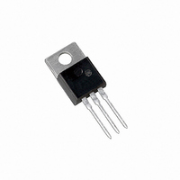
MJE13007G ON Semiconductor, MJE13007G Datasheet - Page 9

MJE13007G
Manufacturer Part Number
MJE13007G
Description
TRANS PWR NPN 8A 400V TO220AB
Manufacturer
ON Semiconductor
Series
SWITCHMODE™r
Type
Powerr
Specifications of MJE13007G
Transistor Type
NPN
Current - Collector (ic) (max)
8A
Voltage - Collector Emitter Breakdown (max)
400V
Vce Saturation (max) @ Ib, Ic
3V @ 2A, 8A
Current - Collector Cutoff (max)
100µA
Dc Current Gain (hfe) (min) @ Ic, Vce
5 @ 5A, 5V
Power - Max
80W
Frequency - Transition
14MHz
Mounting Type
Through Hole
Package / Case
TO-220-3 (Straight Leads)
Transistor Polarity
NPN
Mounting Style
Through Hole
Collector- Emitter Voltage Vceo Max
400 V
Emitter- Base Voltage Vebo
9 V
Maximum Dc Collector Current
8 A
Power Dissipation
80 W
Maximum Operating Temperature
+ 150 C
Continuous Collector Current
8 A
Dc Collector/base Gain Hfe Min
8
Maximum Operating Frequency
14 MHz
Minimum Operating Temperature
- 65 C
Current, Collector
8 A
Current, Gain
30
Frequency
14 MHz
Package Type
TO-220AB
Polarity
NPN
Primary Type
Si
Resistance, Thermal, Junction To Case
1.56 °C/W
Voltage, Breakdown, Collector To Emitter
400 V
Voltage, Collector To Emitter
400 V
Voltage, Collector To Emitter, Saturation
3 V
Voltage, Emitter To Base
9 V
Number Of Elements
1
Collector-emitter Voltage
400V
Emitter-base Voltage
9V
Collector Current (dc) (max)
8A
Dc Current Gain (min)
8
Frequency (max)
14MHz
Operating Temp Range
-65C to 150C
Operating Temperature Classification
Military
Mounting
Through Hole
Pin Count
3 +Tab
Lead Free Status / RoHS Status
Lead free / RoHS Compliant
Other names
MJE13007GOS
A
B
C
D
V
SERIES SWITCHING
REGULATOR
FLYBACK
INVERTER
PUSH−PULL
INVERTER/CONVERTER
SOLENOID DRIVER
V
CC
V
CC
CC
CIRCUIT
N
SOLENOID
V
CC
V
V
O
V
O
O
Table 2. Applications Examples of Switching Circuits
Notes:
Notes:
Notes:
Notes:
16 A
T
8 A
C
16 A
T
T
16 A
8 A
T
8 A
16 A
C
1
1
1
C
1
= 100°C
C
= 100°C
= 100°C
8 A
= 100°C
TURN-ON
+
See AN569 for Pulse Power Derating Procedure.
See AN569 for Pulse Power Derating Procedure.
See AN569 for Pulse Power Derating Procedure.
See AN569 for Pulse Power Derating Procedure.
+
+
+ V
TURN-OFF
CC
TURN-OFF
TURN-ON
V
TURN-ON
TURN-OFF
CC
TURN-OFF
TURN-ON
http://onsemi.com
COLLECTOR VOLTAGE
+ N (V
COLLECTOR VOLTAGE
COLLECTOR VOLTAGE
V
V
CC
CC
LOAD LINE DIAGRAMS
o
V
)
CC
TURN-ON (FORWARD BIAS) SOA
t
DUTY CYCLE ≤ 10%
P
on
TURN-ON (FORWARD BIAS) SOA
t
DUTY CYCLE ≤ 10%
P
D
TURN-ON (FORWARD BIAS) SOA
t
DUTY CYCLE ≤ 10%
P
on
on
400 V
D
TURN-ON (FORWARD BIAS) SOA
t
DUTY CYCLE ≤ 10%
P
D
≤ 10 ms
on
= 3200 W
400 V
400 V
D
≤ 10 ms
= 3200 W
400 V
≤ 10 ms
= 3200 W
9
≤ 10 ms
= 3200 W
COLLECTOR VOLTAGE
300 V
300 V
1
300 V
1
1
300 V
1
V
+ LEAKAGE
CC
2
SPIKE
2
2
+ N (V
2
2 V
700 V
CC
700 V
TURN-OFF (REVERSE BIAS) SOA
1.5 V ≤ V
DUTY CYCLE ≤ 10%
TURN-OFF (REVERSE BIAS) SOA
1.5 V ≤ V
DUTY CYCLE ≤ 10%
o
700 V
700 V
TURN-OFF (REVERSE BIAS) SOA
1.5 V ≤ V
DUTY CYCLE ≤ 10%
TURN-OFF (REVERSE BIAS) SOA
1.5 V ≤ V
DUTY CYCLE ≤ 10%
)
1
1
1
1
BE(off)
BE(off)
BE(off)
BE(off)
≤ 9 V
≤ 9 V
≤ 9 V
≤ 9 V
V
V
N (V
V
CC
I
CC
CE
C
V
V
o
+
I
CE
I
CE
)
C
C
V
2 V
TIME DIAGRAMS
I
CE
C
t
on
CC
V
CC
t
on
V
V
CC
t
on
t
CC
on
LEAKAGE SPIKE
t
off
t
off
t
off
TIME
TIME
t
off
t
t
t
t
t
t
t
t


