2N3055G ON Semiconductor, 2N3055G Datasheet - Page 2
2N3055G
Manufacturer Part Number
2N3055G
Description
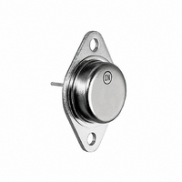
TRANS NPN 15A 60V TO3
Manufacturer
ON Semiconductor
Type
Powerr
Specifications of 2N3055G
Transistor Type
NPN
Current - Collector (ic) (max)
15A
Voltage - Collector Emitter Breakdown (max)
60V
Vce Saturation (max) @ Ib, Ic
3V @ 3.3A, 10A
Current - Collector Cutoff (max)
700µA
Dc Current Gain (hfe) (min) @ Ic, Vce
20 @ 4A, 4V
Power - Max
115W
Frequency - Transition
2.5MHz
Mounting Type
Chassis Mount
Package / Case
TO-204, TO-3
Transistor Polarity
NPN
Mounting Style
Through Hole
Collector- Emitter Voltage Vceo Max
60 V
Emitter- Base Voltage Vebo
7 V
Maximum Dc Collector Current
15 A
Power Dissipation
115000 mW
Maximum Operating Temperature
+ 200 C
Dc Collector/base Gain Hfe Min
20
Maximum Operating Frequency
2.5 MHz
Minimum Operating Temperature
- 65 C
Current, Collector
15 A
Current, Gain
70
Frequency
2.5 MHz
Package Type
TO-204AA (TO-3)
Polarity
NPN
Primary Type
Si
Resistance, Thermal, Junction To Case
1.52 °C/W
Voltage, Breakdown, Collector To Emitter
60 V
Voltage, Collector To Base
100 V
Voltage, Collector To Emitter
60 V
Voltage, Collector To Emitter, Saturation
1.1 V
Voltage, Emitter To Base
7 V
Number Of Elements
1
Collector-emitter Voltage
60V
Collector-base Voltage
100V
Emitter-base Voltage
7V
Collector Current (dc) (max)
15A
Dc Current Gain (min)
20
Frequency (max)
2.5MHz
Operating Temp Range
-65C to 200C
Operating Temperature Classification
Military
Mounting
Through Hole
Pin Count
2 +Tab
Lead Free Status / RoHS Status
Lead free / RoHS Compliant
Other names
2N3055GOS
Available stocks
Company
Part Number
Manufacturer
Quantity
Price

Part Number:
2N3055G
Manufacturer:
ON/安森美
Quantity:
20 000


Î Î Î Î Î Î Î Î Î Î Î Î Î Î Î Î Î Î Î Î Î Î Î Î Î Î Î Î Î Î Î Î Î
Î Î Î Î Î Î Î Î Î Î Î Î Î Î Î Î Î Î Î Î Î Î Î Î Î Î Î Î Î Î Î Î Î
Î Î Î Î Î Î Î Î Î Î Î Î Î Î Î Î Î Î Î Î Î Î Î
Î Î Î Î Î Î Î Î Î Î Î Î Î Î Î Î Î Î Î Î Î Î Î
Î Î Î Î Î Î Î Î Î Î Î Î Î Î Î Î Î Î Î Î Î Î Î
Î Î Î Î Î Î Î Î Î Î Î Î Î Î Î Î Î Î Î Î Î Î Î
Î Î Î Î Î Î Î Î Î Î Î Î Î Î Î Î Î Î Î Î Î Î Î Î Î Î Î Î Î Î Î Î Î
Î Î Î Î Î Î Î Î Î Î Î Î Î Î Î Î Î Î Î Î Î Î Î Î Î Î Î Î Î Î Î Î Î
Î Î Î Î Î Î Î Î Î Î Î Î Î Î Î Î Î Î Î Î Î Î Î
Î Î Î Î Î Î Î Î Î Î Î Î Î Î Î Î Î Î Î Î Î Î Î
Î Î Î Î Î Î Î Î Î Î Î Î Î Î Î Î Î Î Î Î Î Î Î
Î Î Î Î Î Î Î Î Î Î Î Î Î Î Î Î Î Î Î Î Î Î Î
Î Î Î Î Î Î Î Î Î Î Î Î Î Î Î Î Î Î Î Î Î Î Î
Î Î Î Î Î Î Î Î Î Î Î Î Î Î Î Î Î Î Î Î Î Î Î
Î Î Î Î Î Î Î Î Î Î Î Î Î Î Î Î Î Î Î Î Î Î Î
Î Î Î Î Î Î Î Î Î Î Î Î Î Î Î Î Î Î Î Î Î Î Î
Î Î Î Î Î Î Î Î Î Î Î Î Î Î Î Î Î Î Î Î Î Î Î
Î Î Î Î Î Î Î Î Î Î Î Î Î Î Î Î Î Î Î Î Î Î Î Î Î Î Î Î Î Î Î Î Î
Î Î Î Î Î Î Î Î Î Î Î Î Î Î Î Î Î Î Î Î Î Î Î Î Î Î Î Î Î Î Î Î Î
Î Î Î Î Î Î Î Î Î Î Î Î Î Î Î Î Î Î Î Î Î Î Î Î Î Î Î Î Î Î Î Î Î
Î Î Î Î Î Î Î Î Î Î Î Î Î Î Î Î Î Î Î Î Î Î Î Î Î Î Î Î Î Î Î Î Î
Î Î Î Î Î Î Î Î Î Î Î Î Î Î Î Î Î Î Î Î Î Î Î
Î Î Î Î Î Î Î Î Î Î Î Î Î Î Î Î Î Î Î Î Î Î Î
Î Î Î Î Î Î Î Î Î Î Î Î Î Î Î Î Î Î Î Î Î Î Î
Î Î Î Î Î Î Î Î Î Î Î Î Î Î Î Î Î Î Î Î Î Î Î Î Î Î Î Î Î Î Î Î Î
Î Î Î Î Î Î Î Î Î Î Î Î Î Î Î Î Î Î Î Î Î Î Î Î Î Î Î Î Î Î Î Î Î
Î Î Î Î Î Î Î Î Î Î Î Î Î Î Î Î Î Î Î Î Î Î Î
Î Î Î Î Î Î Î Î Î Î Î Î Î Î Î Î Î Î Î Î Î Î Î
Î Î Î Î Î Î Î Î Î Î Î Î Î Î Î Î Î Î Î Î Î Î Î
Î Î Î Î Î Î Î Î Î Î Î Î Î Î Î Î Î Î Î Î Î Î Î
Î Î Î Î Î Î Î Î Î Î Î Î Î Î Î Î Î Î Î Î Î Î Î
Î Î Î Î Î Î Î Î Î Î Î Î Î Î Î Î Î Î Î Î Î Î Î
*Indicates Within JEDEC Registration. (2N3055)
1. Pulse Test: Pulse Width v 300 ms, Duty Cycle v 2.0%.
OFF CHARACTERISTICS*
ON CHARACTERISTICS* (Note 1)
SECOND BREAKDOWN
DYNAMIC CHARACTERISTICS
THERMAL CHARACTERISTICS
ELECTRICAL CHARACTERISTICS
Collector−Emitter Sustaining Voltage (Note 1) (I
Collector−Emitter Sustaining Voltage (Note 1) (I
Collector Cutoff Current (V
Collector Cutoff Current
Emitter Cutoff Current (V
DC Current Gain
Collector−Emitter Saturation Voltage
Base−Emitter On Voltage (I
Second Breakdown Collector Current with Base Forward Biased
Current Gain − Bandwidth Product (I
*Small−Signal Current Gain (I
*Small−Signal Current Gain Cutoff Frequency (V
Thermal Resistance, Junction−to−Case
0.6
0.4
0.2
20
10
6
4
2
1
6
(V
(V
(I
(I
(I
(I
(V
C
C
C
C
Figure 2. Active Region Safe Operating Area
CE
CE
CE
= 4.0 Adc, V
= 10 Adc, V
= 4.0 Adc, I
= 10 Adc, I
V
= 100 Vdc, V
= 100 Vdc, V
CE
= 40 Vdc, t = 1.0 s, Nonrepetitive)
, COLLECTOR−EMITTER VOLTAGE (VOLTS)
BONDING WIRE LIMIT
THERMALLY LIMITED @ T
SECOND BREAKDOWN LIMIT
10
B
B
CE
CE
= 3.3 Adc)
= 400 mAdc)
BE(off)
BE(off)
BE
dc
= 4.0 Vdc)
= 4.0 Vdc)
CE
C
= 7.0 Vdc, I
= 4.0 Adc, V
C
= 30 Vdc, I
= 1.5 Vdc)
= 1.5 Vdc, T
= 1.0 Adc, V
500 ms
20
C
Characteristic
Characteristic
1 ms
= 0.5 Adc, V
C
C
B
= 25°C (SINGLE PULSE)
= 0)
(T
CE
= 0)
C
C
250 ms
CE
= 150°C)
= 4.0 Vdc)
= 25_C unless otherwise noted)
2N3055(NPN), MJ2955(PNP)
= 4.0 Vdc, f = 1.0 kHz)
C
C
CE
= 200 mAdc, I
= 200 mAdc, R
CE
= 4.0 Vdc, I
40
= 10 Vdc, f = 1.0 MHz)
http://onsemi.com
50 ms
60
C
B
BE
= 1.0 Adc, f = 1.0 kHz)
= 0)
2
= 100 W)
a transistor: average junction temperature and second
breakdown. Safe operating area curves indicate I
limits of the transistor that must be observed for reliable
operation; i.e., the transistor must not be subjected to greater
dissipation than the curves indicate.
variable depending on power level. Second breakdown
pulse limits are valid for duty cycles to 10% but must be
derated for temperature according to Figure 1.
There are two limitations on the power handling ability of
The data of Figure 2 is based on T
Î Î Î Î
Î Î Î Î
Î Î Î Î
Î Î Î Î
Î Î Î Î
Î Î Î Î
Î Î Î Î
Î Î Î Î
Î Î Î Î
Î Î Î Î
Î Î Î Î
Î Î Î Î
Î Î Î Î
Î Î Î Î
Î Î Î Î
Î Î Î Î
Î Î Î Î
Î Î Î Î
Î Î Î Î
Î Î Î Î
Î Î Î Î
Î Î Î Î
V
V
Symbol
Symbol
V
V
CEO(sus)
CER(sus)
R
I
CE(sat)
I
I
BE(on)
h
CEO
CEX
EBO
I
f
h
hfe
qJC
s/b
f
FE
T
fe
Î Î Î Î Î Î
Î Î Î Î Î Î
Î Î Î Î Î Î
Î Î Î Î Î Î
Î Î Î Î
Î Î Î Î
Î Î Î Î
Î Î Î Î
Î Î Î Î
Î Î Î Î
Î Î Î Î
Î Î Î Î
Î Î Î Î
Î Î Î Î
Î Î Î Î
Î Î Î Î
Î Î Î Î
Î Î Î Î
Î Î Î Î
Î Î Î Î
Î Î Î Î
Î Î Î Î
2.87
Min
5.0
2.5
60
70
20
15
10
−
−
−
−
−
−
Max
1.52
C
Î Î Î
Î Î Î
Î Î Î
Î Î Î
Î Î Î
Î Î Î
Î Î Î
Î Î Î
Î Î Î
Î Î Î
Î Î Î
Î Î Î
Î Î Î
Î Î Î
Î Î Î
Î Î Î
Î Î Î
Î Î Î
= 25°C; T
Max
120
0.7
1.0
5.0
5.0
1.1
3.0
1.5
70
−
−
−
−
−
−
Î Î Î
Î Î Î
Î Î Î
Î Î Î
Î Î Î
Î Î Î
Î Î Î
Î Î Î
Î Î Î
Î Î Î
Î Î Î
Î Î Î
Î Î Î
Î Î Î
Î Î Î
Î Î Î
Î Î Î
Î Î Î
Î Î Î
Î Î Î
Î Î Î
Î Î Î
C
mAdc
mAdc
mAdc
_C/W
J(pk)
MHz
− V
Unit
Unit
Vdc
Vdc
Vdc
Vdc
Adc
kHz
−
−
CE
is
Related parts for 2N3055G
Image
Part Number
Description
Manufacturer
Datasheet
Request
R

Part Number:
Description:
ON Semiconductor [VOLTAGE REGULATOR]
Manufacturer:
ON Semiconductor
Datasheet:
Part Number:
Description:
357-036-542-201 CARDEDGE 36POS DL .156 BLK LOPRO
Manufacturer:
ON Semiconductor
Datasheet:
Part Number:
Description:
357-036-542-201 CARDEDGE 36POS DL .156 BLK LOPRO
Manufacturer:
ON Semiconductor
Datasheet:
Part Number:
Description:
357-036-542-201 CARDEDGE 36POS DL .156 BLK LOPRO
Manufacturer:
ON Semiconductor
Datasheet:
Part Number:
Description:
357-036-542-201 CARDEDGE 36POS DL .156 BLK LOPRO
Manufacturer:
ON Semiconductor
Datasheet:
Part Number:
Description:
357-036-542-201 CARDEDGE 36POS DL .156 BLK LOPRO
Manufacturer:
ON Semiconductor
Datasheet:
Part Number:
Description:
357-036-542-201 CARDEDGE 36POS DL .156 BLK LOPRO
Manufacturer:
ON Semiconductor
Datasheet:
Part Number:
Description:
357-036-542-201 CARDEDGE 36POS DL .156 BLK LOPRO
Manufacturer:
ON Semiconductor
Datasheet:
Part Number:
Description:
357-036-542-201 CARDEDGE 36POS DL .156 BLK LOPRO
Manufacturer:
ON Semiconductor
Datasheet:
Part Number:
Description:
357-036-542-201 CARDEDGE 36POS DL .156 BLK LOPRO
Manufacturer:
ON Semiconductor
Datasheet:
Part Number:
Description:
357-036-542-201 CARDEDGE 36POS DL .156 BLK LOPRO
Manufacturer:
ON Semiconductor
Datasheet:
Part Number:
Description:
Manufacturer:
ON Semiconductor
Datasheet:
Part Number:
Description:
Manufacturer:
ON Semiconductor
Datasheet:
Part Number:
Description:
Manufacturer:
ON Semiconductor
Datasheet: