PBSS302PX,115 NXP Semiconductors, PBSS302PX,115 Datasheet - Page 5
PBSS302PX,115
Manufacturer Part Number
PBSS302PX,115
Description
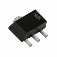
TRANS PNP 20V 5.1A SOT-89
Manufacturer
NXP Semiconductors
Datasheet
1.PBSS302PX115.pdf
(15 pages)
Specifications of PBSS302PX,115
Package / Case
SC-62, SOT-89, TO-243 (3 Leads + Tab)
Transistor Type
PNP
Current - Collector (ic) (max)
5.1A
Voltage - Collector Emitter Breakdown (max)
20V
Vce Saturation (max) @ Ib, Ic
230mV @ 255mA, 5.1A
Dc Current Gain (hfe) (min) @ Ic, Vce
200 @ 2A, 2V
Power - Max
2.1W
Frequency - Transition
130MHz
Mounting Type
Surface Mount
Minimum Operating Temperature
- 65 C
Configuration
Single
Transistor Polarity
PNP
Mounting Style
SMD/SMT
Collector- Emitter Voltage Vceo Max
20 V
Emitter- Base Voltage Vebo
5 V
Maximum Dc Collector Current
5.1 A
Power Dissipation
2100 mW
Maximum Operating Frequency
130 MHz (Typ)
Maximum Operating Temperature
+ 150 C
Lead Free Status / RoHS Status
Lead free / RoHS Compliant
Current - Collector Cutoff (max)
-
Lead Free Status / Rohs Status
Lead free / RoHS Compliant
Other names
568-4174-2
934059015115
PBSS302PX T/R
PBSS302PX T/R
934059015115
PBSS302PX T/R
PBSS302PX T/R


NXP Semiconductors
PBSS302PX_2
Product data sheet
Fig 3.
Fig 4.
Z
Z
(K/W)
(K/W)
th(j-a)
th(j-a)
10
10
10
10
10
10
−1
−1
1
1
2
10
2
10
FR4 PCB, mounting pad for collector 6 cm
Transient thermal impedance from junction to ambient as a function of pulse duration; typical values
Ceramic PCB, Al
Transient thermal impedance from junction to ambient as a function of pulse duration; typical values
−5
−5
δ = 1
0.50
0.20
0.10
0.05
0.02
0.01
δ = 1
0.50
0.20
0.10
0.05
0.02
0.01
0
0
0.75
0.33
0.75
0.33
10
10
−4
−4
2
O
3
, standard footprint
10
10
−3
−3
10
10
2
Rev. 02 — 20 November 2009
−2
−2
10
10
−1
−1
20 V, 5.1 A PNP low V
1
1
10
10
PBSS302PX
CEsat
10
10
2
2
© NXP B.V. 2009. All rights reserved.
(BISS) transistor
t
t
p
p
006aaa558
006aaa559
(s)
(s)
10
10
3
3
5 of 15
Related parts for PBSS302PX,115
Image
Part Number
Description
Manufacturer
Datasheet
Request
R

Part Number:
Description:
NXP Semiconductors designed the LPC2420/2460 microcontroller around a 16-bit/32-bitARM7TDMI-S CPU core with real-time debug interfaces that include both JTAG andembedded trace
Manufacturer:
NXP Semiconductors
Datasheet:

Part Number:
Description:
NXP Semiconductors designed the LPC2458 microcontroller around a 16-bit/32-bitARM7TDMI-S CPU core with real-time debug interfaces that include both JTAG andembedded trace
Manufacturer:
NXP Semiconductors
Datasheet:
Part Number:
Description:
NXP Semiconductors designed the LPC2468 microcontroller around a 16-bit/32-bitARM7TDMI-S CPU core with real-time debug interfaces that include both JTAG andembedded trace
Manufacturer:
NXP Semiconductors
Datasheet:
Part Number:
Description:
NXP Semiconductors designed the LPC2470 microcontroller, powered by theARM7TDMI-S core, to be a highly integrated microcontroller for a wide range ofapplications that require advanced communications and high quality graphic displays
Manufacturer:
NXP Semiconductors
Datasheet:
Part Number:
Description:
NXP Semiconductors designed the LPC2478 microcontroller, powered by theARM7TDMI-S core, to be a highly integrated microcontroller for a wide range ofapplications that require advanced communications and high quality graphic displays
Manufacturer:
NXP Semiconductors
Datasheet:
Part Number:
Description:
The Philips Semiconductors XA (eXtended Architecture) family of 16-bit single-chip microcontrollers is powerful enough to easily handle the requirements of high performance embedded applications, yet inexpensive enough to compete in the market for hi
Manufacturer:
NXP Semiconductors
Datasheet:
Part Number:
Description:
The XA-S3 device is a member of Philips Semiconductors? XA(eXtended Architecture) family of high performance 16-bitsingle-chip microcontrollers
Manufacturer:
NXP Semiconductors
Datasheet:

Part Number:
Description:
The NXP BlueStreak LH75401/LH75411 family consists of two low-cost 16/32-bit System-on-Chip (SoC) devices
Manufacturer:
NXP Semiconductors
Datasheet:
Part Number:
Description:
The NXP LPC3130/3131 combine an 180 MHz ARM926EJ-S CPU core, high-speed USB2
Manufacturer:
NXP Semiconductors
Datasheet:
Part Number:
Description:
The NXP LPC3141 combine a 270 MHz ARM926EJ-S CPU core, High-speed USB 2
Manufacturer:
NXP Semiconductors
Part Number:
Description:
The NXP LPC3143 combine a 270 MHz ARM926EJ-S CPU core, High-speed USB 2
Manufacturer:
NXP Semiconductors

Part Number:
Description:
The NXP LPC3152 combines an 180 MHz ARM926EJ-S CPU core, High-speed USB 2
Manufacturer:
NXP Semiconductors
Part Number:
Description:
The NXP LPC3154 combines an 180 MHz ARM926EJ-S CPU core, High-speed USB 2
Manufacturer:
NXP Semiconductors

Part Number:
Description:
Standard level N-channel enhancement mode Field-Effect Transistor (FET) in a plastic package using NXP High-Performance Automotive (HPA) TrenchMOS technology
Manufacturer:
NXP Semiconductors
Datasheet: