PBSS302PX,115 NXP Semiconductors, PBSS302PX,115 Datasheet - Page 11
PBSS302PX,115
Manufacturer Part Number
PBSS302PX,115
Description
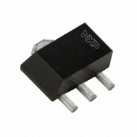
TRANS PNP 20V 5.1A SOT-89
Manufacturer
NXP Semiconductors
Datasheet
1.PBSS302PX115.pdf
(15 pages)
Specifications of PBSS302PX,115
Package / Case
SC-62, SOT-89, TO-243 (3 Leads + Tab)
Transistor Type
PNP
Current - Collector (ic) (max)
5.1A
Voltage - Collector Emitter Breakdown (max)
20V
Vce Saturation (max) @ Ib, Ic
230mV @ 255mA, 5.1A
Dc Current Gain (hfe) (min) @ Ic, Vce
200 @ 2A, 2V
Power - Max
2.1W
Frequency - Transition
130MHz
Mounting Type
Surface Mount
Minimum Operating Temperature
- 65 C
Configuration
Single
Transistor Polarity
PNP
Mounting Style
SMD/SMT
Collector- Emitter Voltage Vceo Max
20 V
Emitter- Base Voltage Vebo
5 V
Maximum Dc Collector Current
5.1 A
Power Dissipation
2100 mW
Maximum Operating Frequency
130 MHz (Typ)
Maximum Operating Temperature
+ 150 C
Lead Free Status / RoHS Status
Lead free / RoHS Compliant
Current - Collector Cutoff (max)
-
Lead Free Status / Rohs Status
Lead free / RoHS Compliant
Other names
568-4174-2
934059015115
PBSS302PX T/R
PBSS302PX T/R
934059015115
PBSS302PX T/R
PBSS302PX T/R


NXP Semiconductors
11. Soldering
PBSS302PX_2
Product data sheet
Fig 16. Reflow soldering footprint SOT89 (SC-62)
Fig 17. Wave soldering footprint SOT89 (SC-62)
4.60
0.85
Not recommended for wave soldering
1.20
1.20
1.00
0.20
(3x)
1.50
3
Rev. 02 — 20 November 2009
6.60
2.40
0.70
5.30
3
3.70
1.90
1.20
3.95
4.75
2.25
2.00
2
1
2
0.50
20 V, 5.1 A PNP low V
1.20
3.50
3.00
1
0.60 (3x)
0.70 (3x)
7.60
0.50
preferred transport direction during soldering
1.20
1.70
4.85
Dimensions in mm
msa442
PBSS302PX
CEsat
solder lands
solder resist
occupied area
Dimensions in mm
© NXP B.V. 2009. All rights reserved.
(BISS) transistor
solder lands
solder resist
occupied area
solder paste
msa423
11 of 15
Related parts for PBSS302PX,115
Image
Part Number
Description
Manufacturer
Datasheet
Request
R

Part Number:
Description:
NXP Semiconductors designed the LPC2420/2460 microcontroller around a 16-bit/32-bitARM7TDMI-S CPU core with real-time debug interfaces that include both JTAG andembedded trace
Manufacturer:
NXP Semiconductors
Datasheet:

Part Number:
Description:
NXP Semiconductors designed the LPC2458 microcontroller around a 16-bit/32-bitARM7TDMI-S CPU core with real-time debug interfaces that include both JTAG andembedded trace
Manufacturer:
NXP Semiconductors
Datasheet:
Part Number:
Description:
NXP Semiconductors designed the LPC2468 microcontroller around a 16-bit/32-bitARM7TDMI-S CPU core with real-time debug interfaces that include both JTAG andembedded trace
Manufacturer:
NXP Semiconductors
Datasheet:
Part Number:
Description:
NXP Semiconductors designed the LPC2470 microcontroller, powered by theARM7TDMI-S core, to be a highly integrated microcontroller for a wide range ofapplications that require advanced communications and high quality graphic displays
Manufacturer:
NXP Semiconductors
Datasheet:
Part Number:
Description:
NXP Semiconductors designed the LPC2478 microcontroller, powered by theARM7TDMI-S core, to be a highly integrated microcontroller for a wide range ofapplications that require advanced communications and high quality graphic displays
Manufacturer:
NXP Semiconductors
Datasheet:
Part Number:
Description:
The Philips Semiconductors XA (eXtended Architecture) family of 16-bit single-chip microcontrollers is powerful enough to easily handle the requirements of high performance embedded applications, yet inexpensive enough to compete in the market for hi
Manufacturer:
NXP Semiconductors
Datasheet:
Part Number:
Description:
The XA-S3 device is a member of Philips Semiconductors? XA(eXtended Architecture) family of high performance 16-bitsingle-chip microcontrollers
Manufacturer:
NXP Semiconductors
Datasheet:

Part Number:
Description:
The NXP BlueStreak LH75401/LH75411 family consists of two low-cost 16/32-bit System-on-Chip (SoC) devices
Manufacturer:
NXP Semiconductors
Datasheet:
Part Number:
Description:
The NXP LPC3130/3131 combine an 180 MHz ARM926EJ-S CPU core, high-speed USB2
Manufacturer:
NXP Semiconductors
Datasheet:
Part Number:
Description:
The NXP LPC3141 combine a 270 MHz ARM926EJ-S CPU core, High-speed USB 2
Manufacturer:
NXP Semiconductors
Part Number:
Description:
The NXP LPC3143 combine a 270 MHz ARM926EJ-S CPU core, High-speed USB 2
Manufacturer:
NXP Semiconductors

Part Number:
Description:
The NXP LPC3152 combines an 180 MHz ARM926EJ-S CPU core, High-speed USB 2
Manufacturer:
NXP Semiconductors
Part Number:
Description:
The NXP LPC3154 combines an 180 MHz ARM926EJ-S CPU core, High-speed USB 2
Manufacturer:
NXP Semiconductors

Part Number:
Description:
Standard level N-channel enhancement mode Field-Effect Transistor (FET) in a plastic package using NXP High-Performance Automotive (HPA) TrenchMOS technology
Manufacturer:
NXP Semiconductors
Datasheet: