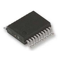
ATA5744N-TKSY 19 Atmel, ATA5744N-TKSY 19 Datasheet - Page 9

ATA5744N-TKSY 19
Manufacturer Part Number
ATA5744N-TKSY 19
Description
RF Receiver RF DATA CONTROL RECEIVER
Manufacturer
Atmel
Type
Receiverr
Datasheet
1.ATA5744N-TKQY.pdf
(20 pages)
Specifications of ATA5744N-TKSY 19
Package / Case
SSO-20
Operating Frequency
449 MHz
Operating Supply Voltage
4.5 V to 5.5 V
Maximum Operating Temperature
+ 105 C
Minimum Operating Temperature
- 40 C
Mounting Style
SMD/SMT
Noise Figure
7 dB
Lead Free Status / RoHS Status
Lead free / RoHS Compliant
4.6
4893A–RKE–11/05
Basic Clock Cycle of the Digital Circuitry
The complete timing of the digital circuitry and the analog filtering is derived from one clock.
According to
bination with a divider. The division factor is controlled by the logical state at pin MODE.
According to chapter 'RF Front End', the frequency of the crystal oscillator (f
the RF input signal (f
Figure 4-3.
Pin MODE can now be set in accordance with the desired clock cycle T
lowing application-relevant parameters:
Timing of the analog and digital signal processing
IF filter center frequency (f
Most applications are dominated by two transmission frequencies: f
used in USA, f
parameters, the electrical characteristics display three conditions for each parameter.
The clock cycle of some function blocks depends on the selected baud rate range (BR_Range)
which is defined by the pins BR_0 and BR_1. This clock cycle T
formulas for further reference:
BR_Range = BR_Range0:
• Application USA
• Application Europe
• Other applications
(f
(f
(T
is given as a function of T
XTO
XTO
Clk
is dependent on f
= 4.90625 MHz, MODE = L, T
= 6.76438 MHz, MODE = H, T
Figure
BR_Range1:
BR_Range2:
BR_Range3:
Generation of the Basic Clock Cycle
Send
= 433.92 MHz in Europe. In order to ease the usage of all T
4-3, this clock cycle TClk is derived from the crystal oscillator (XTO) in com-
RFin
) which also defines the operating frequency of the local oscillator (f
XTO
IF0
)
Clk
and on the logical state of pin MODE. The electrical characteristic
T
T
T
T
).
XClk
XClk
XClk
XClk
:14/:10
Divider
XTO
= 8
= 4
= 2
= 1
T
f
XTO
Clk
Clk
Clk
= 2.0383 µs)
= 2.0697 µs)
T
T
T
T
Clk
Clk
Clk
Clk
16
15
14
MODE
DVCC
XTO
L : USA(:10)
H: Europe(:14)
XClk
is defined by the following
Send
Clk
. T
= 315 MHz is mainly
Clk
XTO
ATA5744
controls the fol-
) is defined by
Clk
-dependent
LO
).
9


