MC12093DR2 ON Semiconductor, MC12093DR2 Datasheet
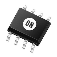
Prescaler 1.1GHz Low Power

MC12093DR2

Manufacturer Part Number
MC12093DR2
Description
Prescaler 1.1GHz Low Power
Manufacturer
ON Semiconductor
Datasheet

Specifications of MC12093DR2

Division
2/4/8
Mounting Style
SMD/SMT
Output Voltage
0.8 V
Package / Case
SOIC-8
Maximum Operating Frequency
1100 MHz
Minimum Operating Frequency
100 MHz
Supply Voltage (min)
2.7 V
Supply Voltage (max)
5.5 V
Operating Supply Voltage
3.3 V, 5 V
Minimum Operating Temperature
- 40 C
Maximum Operating Temperature
+ 85 C
Lead Free Status / RoHS Status
Lead free / RoHS Compliant

Available stocks

Company
Part Number
Manufacturer
Quantity
Price
Part Number:
MC12093DR2
Manufacturer:
NULL
Quantity:
438
Part Number:
MC12093DR2
Manufacturer:
MOTOROLA/摩托罗拉
Quantity:
20 000
Part Number:
MC12093DR2G
Manufacturer:
ON
Quantity:
3 100
Part Number:
MC12093DR2G
Manufacturer:
ON/安森美
Quantity:
20 000
Company:
Part Number:
MC12093DR2G
Quantity:
860
MC12093
÷2, ÷4, ÷8 1.1 GHz Low
Power Prescaler with
Stand-By Mode
Description
frequency division of a 1.1 GHz high frequency input signal.
MOSAIC V™ technology is utilized to achieve low power dissipation
of 6.75 mW at a minimum supply voltage of 2.7 V.
2.0 pF (typical) high impedance load. If additional drive is required
for the prescaler output, an external resistor can be added parallel from
the OUT pin to GND to increase the output power. Care must be taken
not to exceed the maximum allowable current through the output.
ratio of ÷2, ÷4, or ÷8.
when the standby pin SB is switched LOW disabling the prescaler.
Features
Table 1. FUNCTIONAL TABLE
1. SW1 & SW2: H = (V
2. SB: H = 2.0 V to V
© Semiconductor Components Industries, LLC, 2008
August, 2008 − Rev. 7
The MC12093 is a single modulus prescaler for low power
On−chip output termination provides output current to drive a
Divide ratio control inputs SW1 and SW2 select the required divide
Stand−By mode is featured to reduce current drain to 50 mA typical
1.1 GHz Toggle Frequency
Supply Voltage 2.7 V to 5.5 Vdc
Low Power 3.0 mA Typical
Operating Temperature −40°C to 85°C
Divide by 2, 4 or 8 Selected by SW1 and SW2 Pins
On−Chip Termination
Pb−Free Packages are Available
SW
H
H
L
L
Figure 1. Function Chart
CC
CC
, L = GND to 0.8 V.
SW2
H
H
− 0.5 V) to V
L
L
CC
; L = Open.
IN
÷2
÷4
÷8
Divide Ratio
8
4
4
2
1
See detailed ordering and shipping information in the package
dimensions section on page 3 of this data sheet.
A LOW on the Stand−By Pin 7 disables the device.
8
1
ORDERING INFORMATION
A
L
Y
W
G
PIN CONNECTIONS
http://onsemi.com
SW2
OUT
V
CC
IN
= Assembly Location
= Wafer Lot
= Year
= Work Week
= Pb−Free Package
CASE 506AA
MN SUFFIX
CASE 751
D SUFFIX
(Top View)
1
2
3
4
DFN8
SO−8
Publication Order Number:
8
7
6
5
IN
SB
SW1
Gnd
8
1
MARKING
DIAGRAM
1
12093
ALYW
MC12093/D
G
4

Related parts for MC12093DR2

MC12093DR2 Summary of contents

Page 1

... On−chip output termination provides output current to drive a 2.0 pF (typical) high impedance load. If additional drive is required for the prescaler output, an external resistor can be added parallel from the OUT pin to GND to increase the output power. Care must be taken not to exceed the maximum allowable current through the output. ...

Page 2

Table 2. ATTRIBUTES Internal Input Pulldown Resistor Internal Input Pullup Resistor ESD Protection Moisture Sensitivity, Indefinite Time Out of Drypack (Note 1) Flammability Rating Transistor Count Meets or exceeds JEDEC Spec EIA/JESD78 IC Latchup Test 1. For additional information, ...

Page 3

... Input frequency 800−900 MHz, ÷2. 4. Input frequency 900−1100 MHz, ÷2. ORDERING INFORMATION Device MC12093D MC12093DG MC12093DR2 MC12093DR2G MC120932MNR4 MC12093MNR4G †For information on tape and reel specifications, including part orientation and tape sizes, please refer to our Tape and Reel Packaging Specifications Brochure, BRD8011/ 2 − ...

Page 4

... G C SEATING PLANE −Z− 0.25 (0.010 *For additional information on our Pb−Free strategy and soldering details, please download the ON Semiconductor Soldering and Mounting Techniques Reference Manual, SOLDERRM/D. PACKAGE DIMENSIONS SOIC−8 NB CASE 751−07 ISSUE 0.10 (0.004 SOLDERING FOOTPRINT* 1 ...

Page 5

... Opportunity/Affirmative Action Employer. This literature is subject to all applicable copyright laws and is not for resale in any manner. PUBLICATION ORDERING INFORMATION LITERATURE FULFILLMENT: Literature Distribution Center for ON Semiconductor P.O. Box 5163, Denver, Colorado 80217 USA Phone: 303−675−2175 or 800−344−3860 Toll Free USA/Canada Fax: 303− ...

Related keywords