AP504 TriQuint, AP504 Datasheet
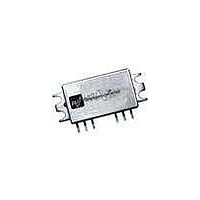
RF Amplifier 1705-790MHz 31.5dB Gain

AP504

Manufacturer Part Number
AP504
Description
RF Amplifier 1705-790MHz 31.5dB Gain
Manufacturer
TriQuint
Type
Power Amplifierr
Datasheet

Specifications of AP504

Operating Frequency
1705 MHz to 1790 MHz
Operating Supply Voltage
12 V
Supply Current
850 mA
Maximum Operating Temperature
+ 85 C
Mounting Style
Through Hole
Minimum Operating Temperature
- 40 C
Number Of Channels
1 Channel
Lead Free Status / RoHS Status
Lead free / RoHS Compliant
WJ Communications, Inc • Phone 1-800-WJ1-4401 • FAX: 408-577-6621 • e-mail: sales@wj.com • Web site: www.wj.com, www.TriQuint.com
Product Features
Applications
Specifications
1. Test conditions unless otherwise noted: 25ºC.
2. The current can be adjusted through an external resistor from the 5V supply to the pull-down voltage pin (pin 3).
Absolute Maximum Rating
Operation of this device above any of these parameters may cause permanent damage.
25 ºC, V
Parameter
Operational Bandwidth
Test Frequency
Adjacent Channel Power Ratio
Power Gain
Input Return Loss
Output Return Loss
Output P1dB
Output IP3
Operating Current
Quiescent Current, Icq
Device Voltage, Vcc
Device Voltage, Vpd
Load Stability
Parameter
Operating Case Temperature
Storage Temperature
RF Input Power (continuous)
1705 – 1790 MHz
31.5 dB Gain
+25 dBm CDMA2k 7fa Power
+12 V Single Supply
Power Down Mode
Bias Current Adjustable
RoHS-compliant flange-mount pkg
Final stage amplifiers for Repeaters
Optimized for driver amplifier PA
mobile infrastructure
with output terminated in 50 Ω
(-63 dBc ACPR)
cc
=12V, V
AP504
DCS-band 4W HBT Amplifier Module
pd
(2)
=5V, I
(2)
cq
(1)
=835mA, R7=0Ω, 50Ω unmatched fixture
Units
VSWR
MHz
MHz
dBm
dBm
dBc
mA
mA
dB
dB
dB
V
V
Rating
-40 to +85 °C
-55 to +150 °C
+15 dBm
The AP504 is a high dynamic range power amplifier in a
RoHS-compliant flange-mount package. The multi-stage
amplifier module has 31.5 dB gain. The module has been
internally optimized for linearity to provide +25 dBm (-63
dBc ACPR) linear power for 7-carrier CDMA2000
applications.
The AP504 uses a high reliability InGaP/GaAs HBT
process technology and does not require any external
matching components. The module operates off of a +12V
supply and does not requiring any negative biasing voltages;
an internal active bias allows the amplifier to maintain high
linearity over temperature. It has the added feature of a
+5V power down control pin. While the module has been
tuned for optimal performance for Class AB applications,
the quiescent current can also be adjusted for Class B
applications through an external resistor. A low-cost metal
housing allows the device to have a low thermal resistance
and achieves over 100 years MTTF. All devices are 100%
RF and DC tested.
The AP504 is targeted for use as a driver or final stage
amplifier in wireless infrastructure where high linearity and
high power is required. This combination makes the device
an excellent candidate for next generation multi-carrier 3G
base stations using the DCS1800 frequency band.
Min
30.5
10:1
790
780
Product Description
1705 – 1790
Typ
1765
-63.2
31.5
+36
+52
850
835
+12
+5
11
5
Max
35.5
940
920
-61
Ordering Information
Part No.
AP504
AP504-PCB
Test Conditions
CDMA2000 7fa 25 dBm Total Power, 885 kHz offset
Pout = +25 dBm
Pout = +23 dBm/tone, Δf = 1 MHz
Pout = +25 dBm
Pull-down voltage: 0V = “OFF”, 5V=”ON”
Specifications and information are subject to change without notice
Description
DCS-band 4W HBT Amplifier Module
Fully-Assembled Evaluation Board
(Class AB configuration, Icq=835mA)
Functional Diagram
Pin No.
Case
2 / 4
3 / 5
1
1
6
2
Top View
3
RF Output
Function
RF Input
Page 1 of 5 July 2008
Ground
4
Vpd
Vcc
5
6

Related parts for AP504

AP504 Summary of contents

Page 1

... MTTF. All devices are 100% RF and DC tested. The AP504 is targeted for use as a driver or final stage amplifier in wireless infrastructure where high linearity and high power is required. This combination makes the device an excellent candidate for next generation multi-carrier 3G base stations using the DCS1800 frequency band ...

Page 2

... Performance Graphs – Class AB Configuration (AP504-PCB) The AP504-PCB and AP504 module is configured for Class AB by default. The resistor – R7 – which sets the current draw for the amplifier is set at 0 Ω in this configuration. Increasing that value will decrease the quiescent and operating current of the amplifier module, as described on the next page ...

Page 3

... AP504 DCS-band 4W HBT Amplifier Module ACPR vs. Output Power CDMA2000 SR1, 1FA , fc=1765 MHz, +25 °C, Vcc=12V, Icq=850mA -60 1.98 MHz offset 885 kHz offset -70 -80 - Total Output Power (dBm) Output Power / Gain vs. Input Power 1765 MHz, +25 °C, Vcc=12V, Icq=850mA 38 Pout Gain Input Power (dBm) WJ Communications, Inc • ...

Page 4

... AP504 DCS-band 4W HBT Amplifier Module The MTTF of the AP504 can be calculated by first determining how much power is being dissipated by the amplifier module. Because the device’s intended application power amplifier pre-driver or final stage output amplifier, the output RF power of the amplifier will help lower the overall power dissipation ...

Page 5

... Outline Drawing The device will be marked with an “AP504” designator with an alphanumeric lot code on the top surface of the package noted as “ABCD” on the drawing. manufacturing date will also be printed as “XXYY”, where the “XX” represents the week number from 1 – 52. ...

Related keywords