BC856BWT1G ON Semiconductor, BC856BWT1G Datasheet

TRANS PNP GP 65V 100MA SOT-323

BC856BWT1G

Manufacturer Part Number
BC856BWT1G
Description
TRANS PNP GP 65V 100MA SOT-323
Manufacturer
ON Semiconductor
Datasheet

Specifications of BC856BWT1G

Transistor Type
PNP
Current - Collector (ic) (max)
100mA
Voltage - Collector Emitter Breakdown (max)
65V
Vce Saturation (max) @ Ib, Ic
650mV @ 5mA, 100mA
Dc Current Gain (hfe) (min) @ Ic, Vce
220 @ 2mA, 5V
Power - Max
150mW
Frequency - Transition
100MHz
Mounting Type
Surface Mount
Package / Case
SC-70-3, SOT-323-3
Configuration
Single
Transistor Polarity
PNP
Mounting Style
SMD/SMT
Collector- Emitter Voltage Vceo Max
65 V
Emitter- Base Voltage Vebo
5 V
Continuous Collector Current
- 0.1 A
Maximum Dc Collector Current
0.1 A
Power Dissipation
150 mW
Maximum Operating Frequency
100 MHz
Maximum Operating Temperature
+ 150 C
Dc Collector/base Gain Hfe Min
150 at 10 uA at 5 V
Minimum Operating Temperature
- 55 C
Number Of Elements
1
Collector-emitter Voltage
65V
Collector-base Voltage
80V
Emitter-base Voltage
5V
Collector Current (dc) (max)
100mA
Dc Current Gain (min)
220
Frequency (max)
100MHz
Operating Temp Range
-55C to 150C
Operating Temperature Classification
Military
Mounting
Surface Mount
Pin Count
3
Package Type
SC-70
Lead Free Status / RoHS Status
Lead free / RoHS Compliant
Current - Collector Cutoff (max)
-
Lead Free Status / Rohs Status
Lead free / RoHS Compliant

Available stocks

Company
Part Number
Manufacturer
Quantity
Price
Part Number:
BC856BWT1G
Manufacturer:
ON Semiconductor
Quantity:
37 652
Part Number:
BC856BWT1G
Manufacturer:
ON Semiconductor
Quantity:
5
Part Number:
BC856BWT1G
Manufacturer:
ON
Quantity:
30 000
Part Number:
BC856BWT1G
Manufacturer:
ON/安森美
Quantity:
20 000
Part Number:
BC856BWT1G
Manufacturer:
ON
Quantity:
10 388
BC856BWT1 Series,
BC857BWT1 Series,
BC858AWT1 Series
General Purpose
Transistors
PNP Silicon
applications. They are housed in the SC- -70/SOT- -323 which is
designed for low power surface mount applications.
Features
Stresses exceeding Maximum Ratings may damage the device. Maximum
Ratings are stress ratings only. Functional operation above the Recommended
Operating Conditions is not implied. Extended exposure to stresses above the
Recommended Operating Conditions may affect device reliability.
1. FR--5 = 1.0 x 0.75 x 0.062 in.
 Semiconductor Components Industries, LLC, 2010
October, 2010 - - Rev. 2
MAXIMUM RATINGS
THERMAL CHARACTERISTICS
Collector-Emitter Voltage
Collector-Base Voltage
Emitter--Base Voltage
Collector Current -- Continuous
Total Device Dissipation FR-- 5 Board,
Thermal Resistance,
Junction and Storage Temperature
These transistors are designed for general purpose amplifier
Compliant
These Devices are Pb- -Free, Halogen Free/BFR Free and are RoHS
(Note 1) T
Junction--to--Ambient
Characteristic
A
= 25C
Rating
(T
A
= 25C unless otherwise noted)
BC856
BC857
BC858
BC856
BC857
BC858
Symbol
Symbol
T
V
V
V
R
J
P
CEO
CBO
EBO
, T
I
θJA
C
D
stg
-- 55 to +150
Value
--100
--5.0
Max
--65
--45
--30
--80
--50
--30
150
883
1
mAdc
C/W
Unit
Unit
mW
C
V
V
V
See detailed ordering and shipping information in the package
dimensions section on page 5 of this data sheet.
*Date Code orientation may vary depending
upon manufacturing location.
(Note: Microdot may be in either location)
1
ORDERING INFORMATION
xx
M
G
2
MARKING DIAGRAM
http://onsemi.com
BASE
= Specific Device Code
= Date Code*
= Pb--Free Package
1
3
1
xx M G
COLLECTOR
Publication Order Number:
SC- -70/SOT- -323
EMITTER
G
3
CASE 419
2
STYLE 3
BC856BWT1/D

Related parts for BC856BWT1G

BC856BWT1G Summary of contents

Page 1

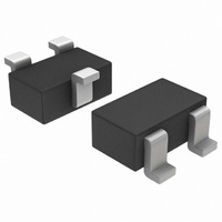
BC856BWT1 Series, BC857BWT1 Series, BC858AWT1 Series General Purpose Transistors PNP Silicon These transistors are designed for general purpose amplifier applications. They are housed in the SC- -70/SOT- -323 which is designed for low power surface mount applications. Features  These ...

Page 2

ELECTRICAL CHARACTERISTICS Characteristic OFF CHARACTERISTICS Collector -- Emitter Breakdown Voltage (I = --10 mA) C Collector -- Emitter Breakdown Voltage (I = --10 mA Collector -- Base Breakdown Voltage (I = --10 mA) C Emitter ...

Page 3

V = -- 25C A 1.0 0.7 0.5 0.3 0.2 --0.2 --0.5 --1.0 --2.0 --5.0 --10 -- COLLECTOR CURRENT (mAdc) C Figure 1. Normalized DC Current Gain --2.0 --1.6 --1 ...

Page 4

V = --5 25C A 2.0 1.0 0.5 0.2 --10 --50 --100 --0.1 --0.2 --1.0 --2.0 --5.0 -- COLLECTOR CURRENT (mA) C Figure 7. DC Current Gain --2.0 --1 --20 mA --50 ...

Page 5

... V , COLLECTOR--EMITTER VOLTAGE (V) CE Figure 14. Active Region Safe Operating Area ORDERING INFORMATION Device BC856BWT1G BC857BWT1G BC857CWT1G BC858AWT1G BC858BWT1G †For information on tape and reel specifications, including part orientation and tape sizes, please refer to our Tape and Reel Packaging Specifications Brochure, BRD8011/D. P ...

Page 6

... A1 *For additional information on our Pb--Free strategy and soldering details, please download the ON Semiconductor Soldering and Mounting Techniques Reference Manual, SOLDERRM/D. ON Semiconductor and are registered trademarks of Semiconductor Components Industries, LLC (SCILLC). SCILLC reserves the right to make changes without further notice to any products herein ...

Related keywords