MJD31CT4G ON Semiconductor, MJD31CT4G Datasheet
MJD31CT4G
Specifications of MJD31CT4G
MJD31CT4GOS
MJD31CT4GOSTR
Available stocks


Related parts for MJD31CT4G


MJD31CT4G Summary of contents
Page 1
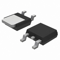
MJD31, MJD31C (NPN), MJD32, MJD32C (PNP) Complementary Power Transistors DPAK For Surface Mount Applications Designed for general purpose amplifier and low speed switching applications. Features • Lead Formed for Surface Mount Applications in Plastic Sleeves • Straight Lead Version in ...
Page 2
ELECTRICAL CHARACTERISTICS Î Î Î Î Î ...
Page 3
2 1 (SURFACE MOUNT 0 100 T, TEMPERATURE (°C) Figure 1. Power Derating ...
Page 4
TYPICAL CHARACTERISTICS − MJD31, MJD31C (NPN) 1000 150°C 25°C 100 −55° 0.01 0 COLLECTOR CURRENT (A) C Figure 6. DC Current Gain 0.5 0.4 0.3 0.2 25°C ...
Page 5
TYPICAL CHARACTERISTICS − MJD31, MJD31C (NPN) 1000 C ib 100 0 REVERSE VOLTAGE (V) R Figure 12. Capacitance 10 1 0.1 0.01 1 100 T = 25° 100 0.001 ...
Page 6
TYPICAL CHARACTERISTICS − MJD32, MJD32C (PNP) 1000 25°C 150°C 100 −55° 0.01 0 COLLECTOR CURRENT (A) C Figure 15. DC Current Gain 0.9 0.8 −55°C 0.7 0.6 ...
Page 7
C ib 100 0 REVERSE VOLTAGE (V) R Figure 21. Capacitance 10 1 0.1 0.01 1 TYPICAL CHARACTERISTICS 100 T = 25° 100 0.001 Figure 22. Current−Gain−Bandwidth Product ...
Page 8
... ORDERING INFORMATION Device MJD31CG MJD31C1G MJD31CRLG MJD31CT4G MJD31T4G MJD32CG MJD32CRLG MJD32CT4 MJD32CT4G MJD32RLG MJD32T4G †For information on tape and reel specifications, including part orientation and tape sizes, please refer to our Tape and Reel Packaging Specifications Brochure, BRD8011/D. Package Type Package DPAK 369C (Pb− ...
Page 9
... DETAIL 0.005 (0.13 0.228 *For additional information on our Pb−Free strategy and soldering details, please download the ON Semiconductor Soldering and Mounting Techniques Reference Manual, SOLDERRM/D. PACKAGE DIMENSIONS DPAK CASE 369C−01 ISSUE GAUGE SEATING L2 C PLANE PLANE DETAIL A ROTATED SOLDERING FOOTPRINT* 6.20 3 ...
Page 10
... Equal Opportunity/Affirmative Action Employer. This literature is subject to all applicable copyright laws and is not for resale in any manner. PUBLICATION ORDERING INFORMATION LITERATURE FULFILLMENT: Literature Distribution Center for ON Semiconductor P.O. Box 5163, Denver, Colorado 80217 USA Phone: 303−675−2175 or 800−344−3860 Toll Free USA/Canada Fax: 303− ...