BDV65B ON Semiconductor, BDV65B Datasheet
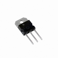
TRANS DARL NPN 100V 10A TO-218

BDV65B

Manufacturer Part Number
BDV65B
Description
TRANS DARL NPN 100V 10A TO-218
Manufacturer
ON Semiconductor
Datasheet

Specifications of BDV65B

Transistor Type
NPN - Darlington
Current - Collector (ic) (max)
10A
Voltage - Collector Emitter Breakdown (max)
100V
Vce Saturation (max) @ Ib, Ic
2V @ 20mA, 5A
Current - Collector Cutoff (max)
1mA
Dc Current Gain (hfe) (min) @ Ic, Vce
1000 @ 5A, 4V
Power - Max
125W
Mounting Type
Through Hole
Package / Case
SOT-93, TO-218 (Straight Leads)
Lead Free Status / RoHS Status
Contains lead / RoHS non-compliant
Frequency - Transition
-

Available stocks

Company
Part Number
Manufacturer
Quantity
Price
Part Number:
BDV65B
Manufacturer:
ST
Quantity:
8 500
Part Number:
BDV65B
Manufacturer:
TOSHIBA
Quantity:
5 000
Part Number:
BDV65B
Manufacturer:
ST
0
Part Number:
BDV65BF
Manufacturer:
ST
0
Part Number:
BDV65BG
Manufacturer:
ON
Quantity:
30 000
Î Î Î Î Î Î Î Î Î Î Î Î Î Î Î Î Î Î Î
Î Î Î Î Î Î Î Î Î Î Î Î Î
Î Î Î Î Î Î Î Î Î Î Î Î Î Î Î Î Î Î Î
Î Î Î Î Î Î Î Î Î Î Î Î Î
BDV65B (NPN),
BDV64B (PNP)
Complementary Silicon
Plastic Power Darlingtons
amplifier applications.
Stresses exceeding Maximum Ratings may damage the device. Maximum
Ratings are stress ratings only. Functional operation above the Recommended
Operating Conditions is not implied. Extended exposure to stresses above the
Recommended Operating Conditions may affect device reliability.
*For additional information on our Pb−Free strategy and soldering details, please
© Semiconductor Components Industries, LLC, 2008
September, 2008 − Rev. 13
MAXIMUM RATINGS
THERMAL CHARACTERISTICS
download the ON Semiconductor Soldering and Mounting Techniques
Reference Manual, SOLDERRM/D.
Collector−Emitter Voltage
Collector−Base Voltage
Emitter−Base Voltage
Collector Current
Base Current
Total Device Dissipation @ T
Derate above 25_C
Operating and Storage Junction Temperature
Range
Thermal Resistance, Junction−to−Case
. . . for use as output devices in complementary general purpose
High DC Current Gain − HFE = 1000 (min.) @ 5 Adc
Monolithic Construction with Built−in Base Emitter Shunt Resistors
Pb−Free Packages are Available*
Characteristic
Rating
− Continuous
− Peak
C
= 25_C
Î Î Î
Î Î Î
Î Î Î
Î Î Î
Î Î Î
Î Î Î
Î Î Î
Î Î Î
Î Î Î
Î Î Î
Î Î Î
Î Î Î
Î Î Î
Î Î Î
Î Î Î
Î Î Î
Î Î Î
Î Î Î
Î Î Î
Î Î Î
Î Î Î
Symbol
Symbol
T
V
R
J
V
V
P
CEO
, T
I
I
qJC
CB
EB
C
B
D
stg
Î Î Î
Î Î Î
Î Î Î
Î Î Î
Î Î Î
Î Î Î
Î Î Î
Î Î Î
Î Î Î
Î Î Î
Î Î Î
Î Î Î
Î Î Î
Î Î Î
Î Î Î
Î Î Î
Î Î Î
Î Î Î
Î Î Î
Î Î Î
Î Î Î
–65 to
+150
Max
Max
100
100
125
5.0
0.5
1.0
1.0
10
20
Î Î Î
Î Î Î
Î Î Î
Î Î Î
Î Î Î
Î Î Î
Î Î Î
Î Î Î
Î Î Î
Î Î Î
Î Î Î
Î Î Î
Î Î Î
Î Î Î
Î Î Î
Î Î Î
Î Î Î
Î Î Î
Î Î Î
Î Î Î
Î Î Î
1
W/_C
_C/W
Unit
Unit
Vdc
Vdc
Vdc
Adc
Adc
_C
W
BDV65B
BDV65BG
BDV64B
BDV64BG
BASE
1
COMPLEMENTARY SILICON
1
10 AMPERE DARLINGTON
Device
2
A
Y
WW
G
BDV6xB
POWER TRANSISTORS
60−80−100−120 VOLTS,
3
ORDERING INFORMATION
COLLECTOR 2
EMITTER 3
BDV65B
NPN
http://onsemi.com
125 WATTS
= Assembly Location
= Year
= Work Week
= Pb−Free Package
= Device Code
CASE 340D
(TO−218)
x = 4 or 5
SOT−93
(Pb−Free)
(Pb−Free)
Package
SOT−93
SOT−93
SOT−93
SOT−93
Publication Order Number:
BASE
1
COLLECTOR 2,4
EMITTER 3
30 Units / Rail
30 Units / Rail
30 Units / Rail
30 Units / Rail
BDV64B
MARKING
DIAGRAM
Shipping
BDV6xBG
PNP
BDV65B/D
AYWW

Related parts for BDV65B

BDV65B Summary of contents

Page 1

... BDV65B (NPN), BDV64B (PNP) Complementary Silicon Plastic Power Darlingtons . . . for use as output devices in complementary general purpose amplifier applications. • High DC Current Gain − HFE = 1000 (min Adc • Monolithic Construction with Built−in Base Emitter Shunt Resistors • Pb−Free Packages are Available* MAXIMUM RATINGS Î ...

Page 2

ELECTRICAL CHARACTERISTICS Î Î Î Î Î ...

Page 3

... I , COLLECTOR CURRENT (A) C Figure 4. “On” Voltages 100 SECONDARY BREAKDOWN v 150°C LIMITED @ T J THERMAL LIMIT @ T = 25° BONDING WIRE LIMIT BDV65B, BDV64B COLLECTOR-EMITTER VOLTAGE (V) CE Figure 6. Active Region Safe Operating Area PNP 10K = 0 0.1 10 0.1 There are two limitations on the power handling ability of 100 μ ...

Page 4

... K 31.00 REF 1.220 REF L --- 16.20 --- 0.638 Q 4.00 4.10 0.158 0.161 S 17.80 18.20 0.701 0.717 U 4.00 REF 0.157 REF V 1.75 REF 0.069 ON Semiconductor Website: www.onsemi.com Order Literature: http://www.onsemi.com/orderlit For additional information, please contact your local Sales Representative BDV65B/D 1000 ...

Related keywords