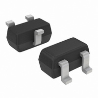
DTA123JET1 ON Semiconductor, DTA123JET1 Datasheet

DTA123JET1
Specifications of DTA123JET1
Related parts for DTA123JET1
DTA123JET1 Summary of contents
Page 1
DTA114EET1 Series Preferred Devices Bias Resistor Transistors PNP Silicon Surface Mount Transistors with Monolithic Bias Resistor Network This new series of digital transistors is designed to replace a single device and its external resistor bias network. The Bias Resistor Transistor ...
Page 2
... DTA123EET1G DTA143EET1 43 DTA143EET1G DTA143ZET1 6K DTA143ZET1G DTA124XET1 6L DTA124XET1G DTA123JET1 6M DTA123JET1G DTA115EET1 6N DTA115EET1G DTA144WET1 6P DTA144WET1G †For information on tape and reel specifications, including part orientation and tape sizes, please refer to our Tape and Reel Packaging Specifications Brochure, BRD8011/D. DTA114EET1 Series R1 (K) R2 (K) Package SC−75 ...
Page 3
... DTA143EET1 DTA143ZET1 DTA124XET1 DTA123JET1 DTA115EET1 DTA144WET1 = 10 mA 0.3 mA) E DTA123EET1 DTA114TET1/DTA143TET1 DTA143ZET1/DTA124XET1 DTA143EET1 DTA114EET1 DTA124EET1 DTA114YET1 DTA114TET1 DTA143TET1 DTA123EET1 DTA143EET1 DTA143ZET1 DTA124XET1 DTA123JET1 DTA144EET1 DTA115EET1 DTA144WET1 http://onsemi.com 3 Symbol Min Typ Max I − − 100 CBO I − − 500 CEO I − ...
Page 4
... L DTA114TET1 DTA143TET1 DTA123EET1 DTA143EET1 DTA114EET1 DTA124EET1 DTA144EET1 DTA114YET1 DTA114TET1 DTA143TET1 DTA123EET1 DTA143EET1 DTA143ZET1 DTA124XET1 DTA123JET1 DTA115EET1 DTA144WET1 DTA114EET1/DTA124EET1 DTA144EET1/DTA115EET1 DTA114YET1 DTA114TET1/DTA143TET1 DTA123EET1/DTA143EET1 DTA143ZET1 DTA124XET1 DTA123JET1 DTA144WET1 http://onsemi.com 4 Symbol Min Typ Max V 4.9 − − 7 15.4 22 28.6 32.9 47 61.1 7 ...
Page 5
D = 0.5 0.2 0.1 0.1 0.05 0.02 0.01 0.01 SINGLE PULSE 0.001 0.00001 0.0001 0.001 Figure 2. Normalized Thermal Response DTA114EET1 Series R = 600°C/W qJA 0 50 100 150 T ...
Page 6
TYPICAL ELECTRICAL CHARACTERISTICS − DTA114EET1 −25°C A 0.1 75°C 0. COLLECTOR CURRENT (mA) C Figure 3. V versus I CE(sat ...
Page 7
TYPICAL ELECTRICAL CHARACTERISTICS − DTA123EET1 0.1 −25°C 25°C 0.01 0.001 COLLECTOR CURRENT (mA) C Figure 8. V versus I CE(sat ...
Page 8
TYPICAL ELECTRICAL CHARACTERISTICS − DTA124EET1 −25°C A 0.1 0. COLLECTOR CURRENT (mA) C Figure 13. V versus I CE(sat ...
Page 9
TYPICAL ELECTRICAL CHARACTERISTICS − DTA144EET1 −25°C A 0.1 0. COLLECTOR CURRENT (mA) C Figure 18. V versus I CE(sat) 1 0.8 0.6 0.4 0 ...
Page 10
TYPICAL ELECTRICAL CHARACTERISTICS − DTA114YET1 0.1 75°C 0.01 0.001 COLLECTOR CURRENT (mA) C Figure 23. V versus I CE(sat) 4.5 4 3.5 3 2.5 2 1.5 1 ...
Page 11
TYPICAL ELECTRICAL CHARACTERISTICS — DTA115EET1 1 0.1 −25°C 0. COLLECTOR CURRENT (mA) C Figure 29. Maximum Collector Voltage versus Collector Current 1.2 1.0 0.8 0.6 0.4 0 ...
Page 12
TYPICAL ELECTRICAL CHARACTERISTICS — DTA144WET1 −25°C A 0.1 25°C 0. COLLECTOR CURRENT (mA) C Figure 34. Maximum Collector Voltage versus Collector Current 1.4 1.2 1.0 0.8 0.6 0.4 ...
Page 13
... *For additional information on our Pb−Free strategy and soldering details, please download the ON Semiconductor Soldering and Mounting Techniques Reference Manual, SOLDERRM/D. ON Semiconductor and are registered trademarks of Semiconductor Components Industries, LLC (SCILLC). SCILLC reserves the right to make changes without further notice to any products herein. SCILLC makes no warranty, representation or guarantee regarding the suitability of its products for any particular purpose, nor does SCILLC assume any liability arising out of the application or use of any product or circuit, and specifically disclaims any and all liability, including without limitation special, consequential or incidental damages. “ ...


