ICS8312AY IDT, Integrated Device Technology Inc, ICS8312AY Datasheet
ICS8312AY
Specifications of ICS8312AY
Available stocks


Related parts for ICS8312AY


ICS8312AY Summary of contents
Page 1
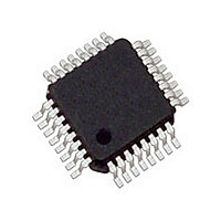
... Available in both standard (RoHS 5) and lead-free (RoHS 6) packages Pin Assignment GND V CLK_EN 12 Q[0:11] CLK GND V GND 7mm x 7mm x 1.4mm package body 1 ICS8312 ICS8312 32-Lead LQFP Y Package Top View ICS8312AY REV. D JULY 3, 2008 Q4 V DDO Q5 GND Q6 V DDO Q7 GND ...
Page 2
... Output Single-ended clock outputs. LVCMOS/LVTTL interface levels. Power Output supply pins. Test Conditions V = 3.465V DDO V = 2.625V DDO DDO V = 3.3V ± 5% DDO V = 2.5V ± 5% DDO V = 1.8V ± 0.2V DDO 2 Minimum Typical Maximum ICS8312AY REV. D JULY 3, 2008 Units pF Ω k Ω Ω Ω Ω ...
Page 3
... Table 3A. Output Enable and Clock Enable Function Table Inputs OE CLK_EN Follows CLK input Table 3B. Output Enable and Clock Enable Function Table Inputs OE CLK_EN IDT™ / ICS™ LVCMOS/LVTTL FANOUT BUFFER Outputs Q [0:11] Hi-Z LOW Outputs CLK Q [0:11] 0 LOW 1 HIGH 3 ICS8312AY REV. D JULY 3, 2008 ...
Page 4
... V = 1.8V ± 0.2V DDO A Test Conditions Minimum 0.5V DDO Typical Maximum 3.3 3.465 3.3 3.465 10 10 Typical Maximum 2.5 2.625 2.5 2.625 0°C to 85°C Typical Maximum 1.6 1.8 2.0 1.6 1.8 2 ICS8312AY REV. D JULY 3, 2008 Units Units Units ...
Page 5
... DDO Test Conditions Minimum 2.375 5 = 0°C to 85°C A Typical Maximum 3.3 3.465 2.5 2.625 0°C to 85°C A Typical Maximum 3.3 3.465 1.6 1.8 2 0°C to 85°C A Typical Maximum 2.5 2.625 1.6 1.8 2 ICS8312AY REV. D JULY 3, 2008 Units Units Units ...
Page 6
... See Parameter Measurement Information, Output Load Test Circuit diagrams. DDO 6 Minimum Typical Maximum 0 0.3 DD 0.65 0 -0.3 1.3 -0.3 0.7 -0.3 0.35*V DD 150 5 -5 -150 2.6 1 – 0 – 0.2 DD 0.5 0.45 0.4 0.35 0.2 ICS8312AY REV. D JULY 3, 2008 Units µA µA µA µ ...
Page 7
... DDO DDO 7 Minimum Typical Maximum Units 1.2 1.9 0.037 200 45 /2. Minimum Typical Maximum Units 1.4 2.3 0.022 200 45 /2. ICS8312AY REV. D JULY 3, 2008 250 MHz 2 125 ps 800 ps 700 /2. DDO 250 MHz 3 ...
Page 8
... DDO DDO 8 Minimum Typical Maximum Units 1.6 3.3 0.172 200 45 /2. = 0°C to 85°C A Minimum Typical Maximum Units 1.4 2.1 0.045 200 45 /2. ICS8312AY REV. D JULY 3, 2008 200 MHz 4 140 ps 2.3 ns 800 /2. DDO 250 MHz 2 ...
Page 9
... DDO DDO 9 = 0°C to 85°C A Minimum Typical Maximum Units 1.4 2.4 0.136 200 45 /2. = 0°C to 85°C A Minimum Typical Maximum Units 1.5 2.6 0.114 200 45 /2. ICS8312AY REV. D JULY 3, 2008 200 MHz 3 145 ps 1.3 ns 700 /2. DDO 200 MHz 3 150 ps 1 ...
Page 10
... Additive Phase Jitter, 3.3V @ 100MHz 12kHz to 20MHz = 0.037ps (typical) Offset from Carrier Frequency (Hz) device. This is illustrated above. The device meets the noise floor of what is shown, but can actually be lower. The phase noise is dependant on the input source and measurement equipment. 10 ICS8312AY REV. D JULY 3, 2008 ...
Page 11
... GND -1.25V±5% 3.3V Core/2.5V LVCMOS Output Load AC Test Circuit 1.6V±5% SCOPE LVCMOS GND V DDO 2 -0.9V±0.1V 2.5V Core/1.8V LVCMOS Output Load AC Test Circuit 11 Qx 1.25V±5% DDO Qx 0.9V±0.1V DDO Qx ICS8312AY REV. D JULY 3, 2008 SCOPE SCOPE V DDO 2 SCOPE V DDO 2 ...
Page 12
... Q0:Q11 t R Output Rise/Fall Time IDT™ / ICS™ LVCMOS/LVTTL FANOUT BUFFER Part 1 Qx Part 2 Qy Part-to-Part Skew Q0:Q11 DDO Output Duty Cycle/Pulse Width/Period 80% 20 DDO 2 V DDO 2 tsk(pp DDO DDO PERIOD t PW odc = t PERIOD ICS8312AY REV. D JULY 3, 2008 V DDO 2 ...
Page 13
... All control pins have internal pull-ups or pull-downs; additional resistance is not required but can be added for additional protection. A 1kΩ resistor can be used. IDT™ / ICS™ LVCMOS/LVTTL FANOUT BUFFER Outputs: LVCMOS Outputs: All unused LVCMOS output can be left floating. There should be no trace attached. 13 ICS8312AY REV. D JULY 3, 2008 ...
Page 14
... NOTE: Most modern PCB design use multi-layered boards. The data in the second row pertains to most designs. Transistor Count The transistor count for ICS8312 is: 339 IDT™ / ICS™ LVCMOS/LVTTL FANOUT BUFFER θ vs. Air Flow JA 0 200 67.8°C/W 55.9°C/W 47.9°C/W 42.1°C/W 14 500 50.1°C/W 39.4°C/W ICS8312AY REV. D JULY 3, 2008 ...
Page 15
... Basic D1 & E1 7.00 Basic D2 & E2 5.60 Ref. e 0.80 Basic L 0.45 0.60 θ 0° ccc N 32 Reference Document: JEDEC Publication 95, MS-026 IDT™ / ICS™ LVCMOS/LVTTL FANOUT BUFFER Maximum 1.60 0.15 1.45 0.45 0.20 0.75 7° 0.10 15 ICS8312AY REV. D JULY 3, 2008 ...
Page 16
... Shipping Packaging 32 Lead LQFP 32 Lead LQFP 1000 Tape & Reel “Lead-Free” 32 Lead LQFP “Lead-Free” 32 Lead LQFP 1000 Tape & Reel 16 Temperature Tray 0°C to 85°C 0°C to 85°C Tray 0°C to 85°C 0°C to 85°C ICS8312AY REV. D JULY 3, 2008 ...
Page 17
... Added Additive Phase Jitter specs to AC Tables. Added Additive Phase Jitter Plot. Added Recommendations for Unused Input & Output Pins section. Updated datasheet to new format. 17 PD. max. current spec to 10µA and DDO 4pF max. to 4pF typical. IN ICS8312AY REV. D JULY 3, 2008 Date 2/25/03 5/17/04 6/14/04 7/3/08 ...
Page 18
ICS8312 LOW SKEW, 1-TO-12 LVCMOS/LVTTL FANOUT BUFFER Contact Information: www.IDT.com Sales 800-345-7015 (inside USA) +408-284-8200 (outside USA) Fax: 408-284-2775 www.IDT.com/go/contactIDT © 2008 Integrated Device Technology, Inc. All rights reserved. Product specifications subject to change without notice. IDT and the IDT ...