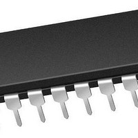
PIC16F1829-E/P Microchip Technology, PIC16F1829-E/P Datasheet - Page 121

PIC16F1829-E/P
Manufacturer Part Number
PIC16F1829-E/P
Description
14 KB Flash, 1K Bytes RAM, 32 MHz Int. Osc, 18 I/0, Enhanced Mid Range Core 20 P
Manufacturer
Microchip Technology
Series
PIC® XLP™ mTouch™ 16Fr
Datasheet
1.PIC16LF1829-ISO.pdf
(420 pages)
Specifications of PIC16F1829-E/P
Core Processor
PIC
Core Size
8-Bit
Speed
32MHz
Connectivity
I²C, LIN, SPI, UART/USART
Peripherals
Brown-out Detect/Reset, POR, PWM, WDT
Number Of I /o
17
Program Memory Size
14KB (8K x 14)
Program Memory Type
FLASH
Eeprom Size
256 x 8
Ram Size
1K x 8
Voltage - Supply (vcc/vdd)
1.8 V ~ 5.5 V
Data Converters
A/D 12x10b
Oscillator Type
Internal
Operating Temperature
-40°C ~ 125°C
Package / Case
*
Processor Series
PIC16F182x
Core
PIC
Data Bus Width
8 bit
Data Ram Size
1 KB
Interface Type
I2C, SPI, USART
Maximum Clock Frequency
32 MHz
Number Of Programmable I/os
18
Number Of Timers
5
Operating Supply Voltage
1.8 V to 5.5 V
Maximum Operating Temperature
+ 125 C
Mounting Style
Through Hole
Lead Free Status / RoHS Status
Lead free / RoHS Compliant
Lead Free Status / RoHS Status
Lead free / RoHS Compliant
- Current page: 121 of 420
- Download datasheet (5Mb)
REGISTER 11-5:
2010 Microchip Technology Inc.
bit 7
Legend:
R = Readable bit
S = Bit can only be set
‘1’ = Bit is set
bit 7
bit 6
bit 5
bit 4
bit 3
bit 2
bit 1
bit 0
R/W-0/0
EEPGD
EEPGD: Flash Program/Data EEPROM Memory Select bit
1 = Accesses program space Flash memory
0 = Accesses data EEPROM memory
CFGS: Flash Program/Data EEPROM or Configuration Select bit
1 = Accesses Configuration, User ID and Device ID Registers
0 = Accesses Flash Program or data EEPROM Memory
LWLO: Load Write Latches Only bit
If CFGS = 1 (Configuration space) OR CFGS = 0 and EEPGD = 1 (program Flash):
If CFGS = 0 and EEPGD = 0: (Accessing data EEPROM)
LWLO is ignored. The next WR command initiates a write to the data EEPROM.
FREE: Program Flash Erase Enable bit
If CFGS = 1 (Configuration space) OR CFGS = 0 and EEPGD = 1 (program Flash):
If EEPGD = 0 and CFGS = 0: (Accessing data EEPROM)
FREE is ignored. The next WR command will initiate both a erase cycle and a write cycle.
WRERR: EEPROM Error Flag bit
1 = Condition indicates an improper program or erase sequence attempt or termination (bit is set
0 = The program or erase operation completed normally.
WREN: Program/Erase Enable bit
1 = Allows program/erase cycles
0 = Inhibits programming/erasing of program Flash and data EEPROM
WR: Write Control bit
1 = Initiates a program Flash or data EEPROM program/erase operation.
0 = Program/erase operation to the Flash or data EEPROM is complete and inactive.
RD: Read Control bit
1 = Initiates an program Flash or data EEPROM read. Read takes one cycle. RD is cleared in
0 = Does not initiate a program Flash or data EEPROM data read.
R/W-0/0
CFGS
1 = The next WR command does not initiate a write; only the program memory latches are
0 = The next WR command writes a value from EEDATH:EEDATL into program memory latches
1 = Performs an erase operation on the next WR command (cleared by hardware after comple-
0 = Performs a write operation on the next WR command.
automatically on any set attempt (write ‘1’) of the WR bit).
The operation is self-timed and the bit is cleared by hardware once operation is complete.
The WR bit can only be set (not cleared) in software.
hardware. The RD bit can only be set (not cleared) in software.
EECON1: EEPROM CONTROL 1 REGISTER
updated.
and initiates a write of all the data stored in the program memory latches.
tion of erase).
W = Writable bit
x = Bit is unknown
‘0’ = Bit is cleared
R/W-0/0
LWLO
R/W/HC-0/0
FREE
Preliminary
U = Unimplemented bit, read as ‘0’
-n/n = Value at POR and BOR/Value at all other Resets
HC = Bit is cleared by hardware
WRERR
R/W-x/q
PIC16F/LF1825/1829
R/W-0/0
WREN
R/S/HC-0/0
WR
DS41440A-page 121
R/S/HC-0/0
RD
bit 0
Related parts for PIC16F1829-E/P
Image
Part Number
Description
Manufacturer
Datasheet
Request
R

Part Number:
Description:
IC, 8BIT MCU, PIC16F, 32MHZ, SOIC-18
Manufacturer:
Microchip Technology
Datasheet:

Part Number:
Description:
IC, 8BIT MCU, PIC16F, 32MHZ, SSOP-20
Manufacturer:
Microchip Technology
Datasheet:

Part Number:
Description:
IC, 8BIT MCU, PIC16F, 32MHZ, DIP-18
Manufacturer:
Microchip Technology
Datasheet:

Part Number:
Description:
IC, 8BIT MCU, PIC16F, 32MHZ, QFN-28
Manufacturer:
Microchip Technology
Datasheet:

Part Number:
Description:
IC, 8BIT MCU, PIC16F, 32MHZ, QFN-28
Manufacturer:
Microchip Technology
Datasheet:

Part Number:
Description:
IC, 8BIT MCU, PIC16F, 32MHZ, QFN-28
Manufacturer:
Microchip Technology
Datasheet:

Part Number:
Description:
IC, 8BIT MCU, PIC16F, 32MHZ, SSOP-20
Manufacturer:
Microchip Technology
Datasheet:

Part Number:
Description:
IC, 8BIT MCU, PIC16F, 20MHZ, DIP-40
Manufacturer:
Microchip Technology
Datasheet:

Part Number:
Description:
IC, 8BIT MCU, PIC16F, 32MHZ, QFN-28
Manufacturer:
Microchip Technology
Datasheet:

Part Number:
Description:
IC, 8BIT MCU, PIC16F, 20MHZ, MQFP-44
Manufacturer:
Microchip Technology
Datasheet:

Part Number:
Description:
IC, 8BIT MCU, PIC16F, 20MHZ, QFN-20
Manufacturer:
Microchip Technology
Datasheet:

Part Number:
Description:
IC, 8BIT MCU, PIC16F, 32MHZ, QFN-28
Manufacturer:
Microchip Technology
Datasheet:

Part Number:
Description:
MCU 14KB FLASH 768B RAM 64-TQFP
Manufacturer:
Microchip Technology
Datasheet:

Part Number:
Description:
7 KB Flash, 384 Bytes RAM, 32 MHz Int. Osc, 16 I/0, Enhanced Mid Range Core, Low
Manufacturer:
Microchip Technology

Part Number:
Description:
14KB Flash, 512B RAM, 256B EEPROM, LCD, 1.8-5.5V 40 UQFN 5x5x0.5mm TUBE
Manufacturer:
Microchip Technology
Datasheet:


