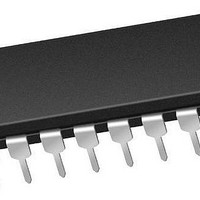
PIC16F1829-E/P Microchip Technology, PIC16F1829-E/P Datasheet - Page 147

PIC16F1829-E/P
Manufacturer Part Number
PIC16F1829-E/P
Description
14 KB Flash, 1K Bytes RAM, 32 MHz Int. Osc, 18 I/0, Enhanced Mid Range Core 20 P
Manufacturer
Microchip Technology
Series
PIC® XLP™ mTouch™ 16Fr
Datasheet
1.PIC16LF1829-ISO.pdf
(420 pages)
Specifications of PIC16F1829-E/P
Core Processor
PIC
Core Size
8-Bit
Speed
32MHz
Connectivity
I²C, LIN, SPI, UART/USART
Peripherals
Brown-out Detect/Reset, POR, PWM, WDT
Number Of I /o
17
Program Memory Size
14KB (8K x 14)
Program Memory Type
FLASH
Eeprom Size
256 x 8
Ram Size
1K x 8
Voltage - Supply (vcc/vdd)
1.8 V ~ 5.5 V
Data Converters
A/D 12x10b
Oscillator Type
Internal
Operating Temperature
-40°C ~ 125°C
Package / Case
*
Processor Series
PIC16F182x
Core
PIC
Data Bus Width
8 bit
Data Ram Size
1 KB
Interface Type
I2C, SPI, USART
Maximum Clock Frequency
32 MHz
Number Of Programmable I/os
18
Number Of Timers
5
Operating Supply Voltage
1.8 V to 5.5 V
Maximum Operating Temperature
+ 125 C
Mounting Style
Through Hole
Lead Free Status / RoHS Status
Lead free / RoHS Compliant
Lead Free Status / RoHS Status
Lead free / RoHS Compliant
- Current page: 147 of 420
- Download datasheet (5Mb)
14.0
The Fixed Voltage Reference, or FVR, is a stable
voltage reference, independent of V
2.048V or 4.096V selectable output levels. The output
of the FVR can be configured to supply a reference
voltage to the following:
• ADC input channel
• ADC positive reference
• Comparator positive input
• Digital-to-Analog Converter (DAC)
The FVR can be enabled by setting the FVREN bit of
the FVRCON register.
FIGURE 14-1:
2010 Microchip Technology Inc.
FIXED VOLTAGE REFERENCE
(FVR)
VOLTAGE REFERENCE BLOCK DIAGRAM
CDAFVR<1:0>
ADFVR<1:0>
FVRRDY
FVREN
DD
, with 1.024V,
2
2
+
_
Preliminary
X
X
X
X
X
X
1.024V Fixed
Reference
1
2
4
1
2
4
14.1
The output of the FVR supplied to the ADC,
Comparators, and DAC is routed through two
independent programmable gain amplifiers. Each
amplifier can be configured to amplify the reference
voltage by 1x, 2x or 4x, to produce the three possible
voltage levels.
The ADFVR<1:0> bits of the FVRCON register are
used to enable and configure the gain amplifier settings
for the reference supplied to the ADC module. Refer-
ence
(ADC) Module”
The CDAFVR<1:0> bits of the FVRCON register are
used to enable and configure the gain amplifier settings
for the reference supplied to the DAC and comparator
module. Reference
Converter (DAC) Module”
parator Module”
14.2
When the Fixed Voltage Reference module is enabled, it
requires time for the reference and amplifier circuits to
stabilize. Once the circuits stabilize and are ready for use,
the FVRRDY bit of the FVRCON register will be set. See
Section 30.0 “Electrical Specifications”
minimum delay requirement.
PIC16F/LF1825/1829
Section 16.0 “Analog-to-Digital Converter
Independent Gain Amplifiers
FVR Stabilization Period
(To Comparators, DAC)
(To ADC Module)
FVR BUFFER1
FVR BUFFER2
for additional information.
for additional information.
Section 17.0 “Digital-to-Analog
and
Section 19.0 “Com-
DS41440A-page 147
for the
Related parts for PIC16F1829-E/P
Image
Part Number
Description
Manufacturer
Datasheet
Request
R

Part Number:
Description:
IC, 8BIT MCU, PIC16F, 32MHZ, SOIC-18
Manufacturer:
Microchip Technology
Datasheet:

Part Number:
Description:
IC, 8BIT MCU, PIC16F, 32MHZ, SSOP-20
Manufacturer:
Microchip Technology
Datasheet:

Part Number:
Description:
IC, 8BIT MCU, PIC16F, 32MHZ, DIP-18
Manufacturer:
Microchip Technology
Datasheet:

Part Number:
Description:
IC, 8BIT MCU, PIC16F, 32MHZ, QFN-28
Manufacturer:
Microchip Technology
Datasheet:

Part Number:
Description:
IC, 8BIT MCU, PIC16F, 32MHZ, QFN-28
Manufacturer:
Microchip Technology
Datasheet:

Part Number:
Description:
IC, 8BIT MCU, PIC16F, 32MHZ, QFN-28
Manufacturer:
Microchip Technology
Datasheet:

Part Number:
Description:
IC, 8BIT MCU, PIC16F, 32MHZ, SSOP-20
Manufacturer:
Microchip Technology
Datasheet:

Part Number:
Description:
IC, 8BIT MCU, PIC16F, 20MHZ, DIP-40
Manufacturer:
Microchip Technology
Datasheet:

Part Number:
Description:
IC, 8BIT MCU, PIC16F, 32MHZ, QFN-28
Manufacturer:
Microchip Technology
Datasheet:

Part Number:
Description:
IC, 8BIT MCU, PIC16F, 20MHZ, MQFP-44
Manufacturer:
Microchip Technology
Datasheet:

Part Number:
Description:
IC, 8BIT MCU, PIC16F, 20MHZ, QFN-20
Manufacturer:
Microchip Technology
Datasheet:

Part Number:
Description:
IC, 8BIT MCU, PIC16F, 32MHZ, QFN-28
Manufacturer:
Microchip Technology
Datasheet:

Part Number:
Description:
MCU 14KB FLASH 768B RAM 64-TQFP
Manufacturer:
Microchip Technology
Datasheet:

Part Number:
Description:
7 KB Flash, 384 Bytes RAM, 32 MHz Int. Osc, 16 I/0, Enhanced Mid Range Core, Low
Manufacturer:
Microchip Technology

Part Number:
Description:
14KB Flash, 512B RAM, 256B EEPROM, LCD, 1.8-5.5V 40 UQFN 5x5x0.5mm TUBE
Manufacturer:
Microchip Technology
Datasheet:


