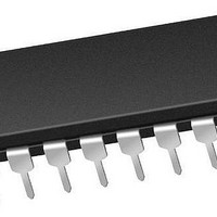
PIC16F1829-E/P Microchip Technology, PIC16F1829-E/P Datasheet - Page 171

PIC16F1829-E/P
Manufacturer Part Number
PIC16F1829-E/P
Description
14 KB Flash, 1K Bytes RAM, 32 MHz Int. Osc, 18 I/0, Enhanced Mid Range Core 20 P
Manufacturer
Microchip Technology
Series
PIC® XLP™ mTouch™ 16Fr
Datasheet
1.PIC16LF1829-ISO.pdf
(420 pages)
Specifications of PIC16F1829-E/P
Core Processor
PIC
Core Size
8-Bit
Speed
32MHz
Connectivity
I²C, LIN, SPI, UART/USART
Peripherals
Brown-out Detect/Reset, POR, PWM, WDT
Number Of I /o
17
Program Memory Size
14KB (8K x 14)
Program Memory Type
FLASH
Eeprom Size
256 x 8
Ram Size
1K x 8
Voltage - Supply (vcc/vdd)
1.8 V ~ 5.5 V
Data Converters
A/D 12x10b
Oscillator Type
Internal
Operating Temperature
-40°C ~ 125°C
Package / Case
*
Processor Series
PIC16F182x
Core
PIC
Data Bus Width
8 bit
Data Ram Size
1 KB
Interface Type
I2C, SPI, USART
Maximum Clock Frequency
32 MHz
Number Of Programmable I/os
18
Number Of Timers
5
Operating Supply Voltage
1.8 V to 5.5 V
Maximum Operating Temperature
+ 125 C
Mounting Style
Through Hole
Lead Free Status / RoHS Status
Lead free / RoHS Compliant
Lead Free Status / RoHS Status
Lead free / RoHS Compliant
- Current page: 171 of 420
- Download datasheet (5Mb)
18.0
The module consists of a single SR Latch with multiple
Set and Reset inputs as well as separate latch outputs.
The SR Latch module includes the following features:
• Programmable input selection
• SR Latch output is available externally
• Separate Q and Q outputs
• Firmware Set and Reset
The SR Latch can be used in a variety of analog appli-
cations, including oscillator circuits, one-shot circuit,
hysteretic controllers, and analog timing applications.
18.1
The latch is a Set-Reset Latch that does not depend on
a clock source. Each of the Set and Reset inputs are
active-high. The latch can be Set or Reset by:
• Software control (SRPS and SRPR bits)
• Comparator C1 output (SYNCC1OUT)
• Comparator C2 output (SYNCC2OUT)
• SRI pin
• Programmable clock (SRCLK)
The SRPS and the SRPR bits of the SRCON0 register
may be used to Set or Reset the SR Latch, respec-
tively. The latch is Reset-dominant. Therefore, if both
Set and Reset inputs are high, the latch will go to the
Reset state. Both the SRPS and SRPR bits are self
resetting which means that a single write to either of the
bits is all that is necessary to complete a latch Set or
Reset operation.
The output from Comparator C1 or C2 can be used as
the Set or Reset inputs of the SR Latch. The output of
either Comparator can be synchronized to the Timer1
clock
Module”
Gate Control”
An external source on the SRI pin can be used as the
Set or Reset inputs of the SR Latch.
An internal clock source is available that can periodically
Set or Reset the SR Latch. The SRCLK<2:0> bits in the
SRCON0 register are used to select the clock source
period. The SRSCKE and SRRCKE bits of the SRCON1
register enable the clock source to Set or Reset the SR
Latch, respectively.
2010 Microchip Technology Inc.
(PIC16F/LF1829 only)
Note:
source.
SR LATCH
Latch Operation
and
Enabling both the Set and Reset inputs
from any one source at the same time
may result in indeterminate operation, as
the Reset dominance cannot be assured.
for more information.
Section 21.0 “Timer1 Module with
See
Section 19.0
“Comparator
Preliminary
18.2
The SRQEN and SRNQEN bits of the SRCON0 regis-
ter control the Q and Q latch outputs. Both of the SR
Latch outputs may be directly output to an I/O pin at the
same time.
The applicable TRIS bit of the corresponding port must
be cleared to enable the port pin output driver.
18.3
Upon any device Reset, the SR Latch output is not ini-
tialized to a known state. The user’s firmware is
responsible for initializing the latch output before
enabling the output pins.
PIC16F/LF1825/1829
Latch Output
Effects of a Reset
DS41440A-page 171
Related parts for PIC16F1829-E/P
Image
Part Number
Description
Manufacturer
Datasheet
Request
R

Part Number:
Description:
IC, 8BIT MCU, PIC16F, 32MHZ, SOIC-18
Manufacturer:
Microchip Technology
Datasheet:

Part Number:
Description:
IC, 8BIT MCU, PIC16F, 32MHZ, SSOP-20
Manufacturer:
Microchip Technology
Datasheet:

Part Number:
Description:
IC, 8BIT MCU, PIC16F, 32MHZ, DIP-18
Manufacturer:
Microchip Technology
Datasheet:

Part Number:
Description:
IC, 8BIT MCU, PIC16F, 32MHZ, QFN-28
Manufacturer:
Microchip Technology
Datasheet:

Part Number:
Description:
IC, 8BIT MCU, PIC16F, 32MHZ, QFN-28
Manufacturer:
Microchip Technology
Datasheet:

Part Number:
Description:
IC, 8BIT MCU, PIC16F, 32MHZ, QFN-28
Manufacturer:
Microchip Technology
Datasheet:

Part Number:
Description:
IC, 8BIT MCU, PIC16F, 32MHZ, SSOP-20
Manufacturer:
Microchip Technology
Datasheet:

Part Number:
Description:
IC, 8BIT MCU, PIC16F, 20MHZ, DIP-40
Manufacturer:
Microchip Technology
Datasheet:

Part Number:
Description:
IC, 8BIT MCU, PIC16F, 32MHZ, QFN-28
Manufacturer:
Microchip Technology
Datasheet:

Part Number:
Description:
IC, 8BIT MCU, PIC16F, 20MHZ, MQFP-44
Manufacturer:
Microchip Technology
Datasheet:

Part Number:
Description:
IC, 8BIT MCU, PIC16F, 20MHZ, QFN-20
Manufacturer:
Microchip Technology
Datasheet:

Part Number:
Description:
IC, 8BIT MCU, PIC16F, 32MHZ, QFN-28
Manufacturer:
Microchip Technology
Datasheet:

Part Number:
Description:
MCU 14KB FLASH 768B RAM 64-TQFP
Manufacturer:
Microchip Technology
Datasheet:

Part Number:
Description:
7 KB Flash, 384 Bytes RAM, 32 MHz Int. Osc, 16 I/0, Enhanced Mid Range Core, Low
Manufacturer:
Microchip Technology

Part Number:
Description:
14KB Flash, 512B RAM, 256B EEPROM, LCD, 1.8-5.5V 40 UQFN 5x5x0.5mm TUBE
Manufacturer:
Microchip Technology
Datasheet:


