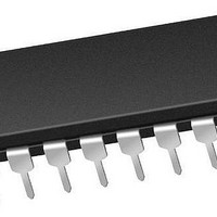
PIC16F1829-E/P Microchip Technology, PIC16F1829-E/P Datasheet - Page 185

PIC16F1829-E/P
Manufacturer Part Number
PIC16F1829-E/P
Description
14 KB Flash, 1K Bytes RAM, 32 MHz Int. Osc, 18 I/0, Enhanced Mid Range Core 20 P
Manufacturer
Microchip Technology
Series
PIC® XLP™ mTouch™ 16Fr
Datasheet
1.PIC16LF1829-ISO.pdf
(420 pages)
Specifications of PIC16F1829-E/P
Core Processor
PIC
Core Size
8-Bit
Speed
32MHz
Connectivity
I²C, LIN, SPI, UART/USART
Peripherals
Brown-out Detect/Reset, POR, PWM, WDT
Number Of I /o
17
Program Memory Size
14KB (8K x 14)
Program Memory Type
FLASH
Eeprom Size
256 x 8
Ram Size
1K x 8
Voltage - Supply (vcc/vdd)
1.8 V ~ 5.5 V
Data Converters
A/D 12x10b
Oscillator Type
Internal
Operating Temperature
-40°C ~ 125°C
Package / Case
*
Processor Series
PIC16F182x
Core
PIC
Data Bus Width
8 bit
Data Ram Size
1 KB
Interface Type
I2C, SPI, USART
Maximum Clock Frequency
32 MHz
Number Of Programmable I/os
18
Number Of Timers
5
Operating Supply Voltage
1.8 V to 5.5 V
Maximum Operating Temperature
+ 125 C
Mounting Style
Through Hole
Lead Free Status / RoHS Status
Lead free / RoHS Compliant
Lead Free Status / RoHS Status
Lead free / RoHS Compliant
- Current page: 185 of 420
- Download datasheet (5Mb)
20.0
The Timer0 module is an 8-bit timer/counter with the
following features:
• 8-bit timer/counter register (TMR0)
• 8-bit prescaler (independent of Watchdog Timer)
• Programmable internal or external clock source
• Programmable external clock edge selection
• Interrupt on overflow
• TMR0 can be used to gate Timer1
Figure 20-1
20.1
The Timer0 module can be used as either an 8-bit timer
or an 8-bit counter.
20.1.1
The Timer0 module will increment every instruction
cycle, if used without a prescaler. 8-bit Timer mode is
selected by clearing the TMR0CS bit of the OPTION
register.
When TMR0 is written, the increment is inhibited for
two instruction cycles immediately following the write.
FIGURE 20-1:
2010 Microchip Technology Inc.
From CPSCLK
Note:
T0CKI
F
OSC
TIMER0 MODULE
Timer0 Operation
/4
8-BIT TIMER MODE
The value written to the TMR0 register
can be adjusted, in order to account for
the two instruction cycle delay when
TMR0 is written.
is a block diagram of the Timer0 module.
T0XCS
0
1
TMR0SE
BLOCK DIAGRAM OF THE TIMER0
TMR0CS
0
1
Preliminary
Prescaler
8-bit
8
PS<2:0>
20.1.2
In 8-Bit Counter mode, the Timer0 module will increment
on every rising or falling edge of the T0CKI pin or the
Capacitive Sensing Oscillator (CPSCLK) signal.
8-Bit Counter mode using the T0CKI pin is selected by
setting the TMR0CS bit in the OPTION register to ‘1’
and resetting the T0XCS bit in the CPSCON0 register to
‘0’.
8-Bit Counter mode using the Capacitive Sensing
Oscillator (CPSCLK) signal is selected by setting the
TMR0CS bit in the OPTION register to ‘1’ and setting
the T0XCS bit in the CPSCON0 register to ‘1’.
The rising or falling transition of the incrementing edge
for either input source is determined by the TMR0SE bit
in the OPTION register.
PIC16F/LF1825/1829
8-BIT COUNTER MODE
PSA
1
0
2 T
Sync
CY
Set Flag bit TMR0IF
DS41440A-page 187
Overflow to Timer1
on Overflow
Data Bus
8
TMR0
Related parts for PIC16F1829-E/P
Image
Part Number
Description
Manufacturer
Datasheet
Request
R

Part Number:
Description:
IC, 8BIT MCU, PIC16F, 32MHZ, SOIC-18
Manufacturer:
Microchip Technology
Datasheet:

Part Number:
Description:
IC, 8BIT MCU, PIC16F, 32MHZ, SSOP-20
Manufacturer:
Microchip Technology
Datasheet:

Part Number:
Description:
IC, 8BIT MCU, PIC16F, 32MHZ, DIP-18
Manufacturer:
Microchip Technology
Datasheet:

Part Number:
Description:
IC, 8BIT MCU, PIC16F, 32MHZ, QFN-28
Manufacturer:
Microchip Technology
Datasheet:

Part Number:
Description:
IC, 8BIT MCU, PIC16F, 32MHZ, QFN-28
Manufacturer:
Microchip Technology
Datasheet:

Part Number:
Description:
IC, 8BIT MCU, PIC16F, 32MHZ, QFN-28
Manufacturer:
Microchip Technology
Datasheet:

Part Number:
Description:
IC, 8BIT MCU, PIC16F, 32MHZ, SSOP-20
Manufacturer:
Microchip Technology
Datasheet:

Part Number:
Description:
IC, 8BIT MCU, PIC16F, 20MHZ, DIP-40
Manufacturer:
Microchip Technology
Datasheet:

Part Number:
Description:
IC, 8BIT MCU, PIC16F, 32MHZ, QFN-28
Manufacturer:
Microchip Technology
Datasheet:

Part Number:
Description:
IC, 8BIT MCU, PIC16F, 20MHZ, MQFP-44
Manufacturer:
Microchip Technology
Datasheet:

Part Number:
Description:
IC, 8BIT MCU, PIC16F, 20MHZ, QFN-20
Manufacturer:
Microchip Technology
Datasheet:

Part Number:
Description:
IC, 8BIT MCU, PIC16F, 32MHZ, QFN-28
Manufacturer:
Microchip Technology
Datasheet:

Part Number:
Description:
MCU 14KB FLASH 768B RAM 64-TQFP
Manufacturer:
Microchip Technology
Datasheet:

Part Number:
Description:
7 KB Flash, 384 Bytes RAM, 32 MHz Int. Osc, 16 I/0, Enhanced Mid Range Core, Low
Manufacturer:
Microchip Technology

Part Number:
Description:
14KB Flash, 512B RAM, 256B EEPROM, LCD, 1.8-5.5V 40 UQFN 5x5x0.5mm TUBE
Manufacturer:
Microchip Technology
Datasheet:


