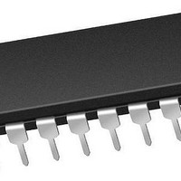
PIC16F1829-E/P Microchip Technology, PIC16F1829-E/P Datasheet - Page 205

PIC16F1829-E/P
Manufacturer Part Number
PIC16F1829-E/P
Description
14 KB Flash, 1K Bytes RAM, 32 MHz Int. Osc, 18 I/0, Enhanced Mid Range Core 20 P
Manufacturer
Microchip Technology
Series
PIC® XLP™ mTouch™ 16Fr
Datasheet
1.PIC16LF1829-ISO.pdf
(420 pages)
Specifications of PIC16F1829-E/P
Core Processor
PIC
Core Size
8-Bit
Speed
32MHz
Connectivity
I²C, LIN, SPI, UART/USART
Peripherals
Brown-out Detect/Reset, POR, PWM, WDT
Number Of I /o
17
Program Memory Size
14KB (8K x 14)
Program Memory Type
FLASH
Eeprom Size
256 x 8
Ram Size
1K x 8
Voltage - Supply (vcc/vdd)
1.8 V ~ 5.5 V
Data Converters
A/D 12x10b
Oscillator Type
Internal
Operating Temperature
-40°C ~ 125°C
Package / Case
*
Processor Series
PIC16F182x
Core
PIC
Data Bus Width
8 bit
Data Ram Size
1 KB
Interface Type
I2C, SPI, USART
Maximum Clock Frequency
32 MHz
Number Of Programmable I/os
18
Number Of Timers
5
Operating Supply Voltage
1.8 V to 5.5 V
Maximum Operating Temperature
+ 125 C
Mounting Style
Through Hole
Lead Free Status / RoHS Status
Lead free / RoHS Compliant
Lead Free Status / RoHS Status
Lead free / RoHS Compliant
- Current page: 205 of 420
- Download datasheet (5Mb)
23.0
The Data Signal Modulator (DSM) is a peripheral which
allows the user to mix a data stream, also known as a
modulator signal, with a carrier signal to produce a
modulated output.
Both the carrier and the modulator signals are supplied
to the DSM module either internally, from the output of
a peripheral, or externally through an input pin.
The modulated output signal is generated by perform-
ing a logical “AND” operation of both the carrier and
modulator signals and then provided to the MDOUT pin.
The carrier signal is comprised of two distinct and sep-
arate signals. A carrier high (CARH) signal and a car-
rier low (CARL) signal. During the time in which the
modulator (MOD) signal is in a logic high state, the
DSM mixes the carrier high signal with the modulator
signal. When the modulator signal is in a logic low
state, the DSM mixes the carrier low signal with the
modulator signal.
FIGURE 23-1:
2010 Microchip Technology Inc.
Comparator C1
Comparator C2
MSSP1 SDO1
MSSP2 SDO2
MDCL<3:0>
DATA SIGNAL MODULATOR
MDCH<3:0>
MDMS<3:0>
No Channel
No Channel
No Channel
EUSART
MDCIN1
MDCIN2
MDCIN1
MDCIN2
Reserved
Reserved
Reserved
MDMIN
Selected
Selected
Selected
MDBIT
CLKR
CCP1
CCP2
CCP3
CCP4
CCP1
CCP2
CCP3
CCP4
CLKR
CCP1
CCP2
CCP3
CCP4
V
V
SS
SS
SIMPLIFIED BLOCK DIAGRAM OF THE DATA SIGNAL MODULATOR
0000
0001
0010
0011
0100
0000
0001
0010
0011
0100
*
*
0000
0001
0010
0011
0100
0101
0110
0111
1000
*
*
1111
0101
0110
0111
1000
1001
1010
0011
1111
0101
0110
0111
1000
*
*
1111
CARH
MOD
CARL
MDCHPOL
MDCLPOL
MDEN
EN
Preliminary
D
D
SYNC
SYNC
Data Signal
Modulator
Q
Q
MDCLSYNC
Using this method, the DSM can generate the following
types of Key Modulation schemes:
• Frequency-Shift Keying (FSK)
• Phase-Shift Keying (PSK)
• On-Off Keying (OOK)
Additionally, the following features are provided within
the DSM module:
• Carrier Synchronization
• Carrier Source Polarity Select
• Carrier Source Pin Disable
• Programmable Modulator Data
• Modulator Source Pin Disable
• Modulated Output Polarity Select
• Slew Rate Control
Figure 23-1
Data Signal Modulator peripheral.
PIC16F/LF1825/1829
MDCHSYNC
1
0
1
0
shows a Simplified Block Diagram of the
MDOPOL
MDOE
DS41440A-page 207
MDOUT
Related parts for PIC16F1829-E/P
Image
Part Number
Description
Manufacturer
Datasheet
Request
R

Part Number:
Description:
IC, 8BIT MCU, PIC16F, 32MHZ, SOIC-18
Manufacturer:
Microchip Technology
Datasheet:

Part Number:
Description:
IC, 8BIT MCU, PIC16F, 32MHZ, SSOP-20
Manufacturer:
Microchip Technology
Datasheet:

Part Number:
Description:
IC, 8BIT MCU, PIC16F, 32MHZ, DIP-18
Manufacturer:
Microchip Technology
Datasheet:

Part Number:
Description:
IC, 8BIT MCU, PIC16F, 32MHZ, QFN-28
Manufacturer:
Microchip Technology
Datasheet:

Part Number:
Description:
IC, 8BIT MCU, PIC16F, 32MHZ, QFN-28
Manufacturer:
Microchip Technology
Datasheet:

Part Number:
Description:
IC, 8BIT MCU, PIC16F, 32MHZ, QFN-28
Manufacturer:
Microchip Technology
Datasheet:

Part Number:
Description:
IC, 8BIT MCU, PIC16F, 32MHZ, SSOP-20
Manufacturer:
Microchip Technology
Datasheet:

Part Number:
Description:
IC, 8BIT MCU, PIC16F, 20MHZ, DIP-40
Manufacturer:
Microchip Technology
Datasheet:

Part Number:
Description:
IC, 8BIT MCU, PIC16F, 32MHZ, QFN-28
Manufacturer:
Microchip Technology
Datasheet:

Part Number:
Description:
IC, 8BIT MCU, PIC16F, 20MHZ, MQFP-44
Manufacturer:
Microchip Technology
Datasheet:

Part Number:
Description:
IC, 8BIT MCU, PIC16F, 20MHZ, QFN-20
Manufacturer:
Microchip Technology
Datasheet:

Part Number:
Description:
IC, 8BIT MCU, PIC16F, 32MHZ, QFN-28
Manufacturer:
Microchip Technology
Datasheet:

Part Number:
Description:
MCU 14KB FLASH 768B RAM 64-TQFP
Manufacturer:
Microchip Technology
Datasheet:

Part Number:
Description:
7 KB Flash, 384 Bytes RAM, 32 MHz Int. Osc, 16 I/0, Enhanced Mid Range Core, Low
Manufacturer:
Microchip Technology

Part Number:
Description:
14KB Flash, 512B RAM, 256B EEPROM, LCD, 1.8-5.5V 40 UQFN 5x5x0.5mm TUBE
Manufacturer:
Microchip Technology
Datasheet:


