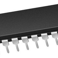
PIC16F1829-E/P Microchip Technology, PIC16F1829-E/P Datasheet - Page 206

PIC16F1829-E/P
Manufacturer Part Number
PIC16F1829-E/P
Description
14 KB Flash, 1K Bytes RAM, 32 MHz Int. Osc, 18 I/0, Enhanced Mid Range Core 20 P
Manufacturer
Microchip Technology
Series
PIC® XLP™ mTouch™ 16Fr
Datasheet
1.PIC16LF1829-ISO.pdf
(420 pages)
Specifications of PIC16F1829-E/P
Core Processor
PIC
Core Size
8-Bit
Speed
32MHz
Connectivity
I²C, LIN, SPI, UART/USART
Peripherals
Brown-out Detect/Reset, POR, PWM, WDT
Number Of I /o
17
Program Memory Size
14KB (8K x 14)
Program Memory Type
FLASH
Eeprom Size
256 x 8
Ram Size
1K x 8
Voltage - Supply (vcc/vdd)
1.8 V ~ 5.5 V
Data Converters
A/D 12x10b
Oscillator Type
Internal
Operating Temperature
-40°C ~ 125°C
Package / Case
*
Processor Series
PIC16F182x
Core
PIC
Data Bus Width
8 bit
Data Ram Size
1 KB
Interface Type
I2C, SPI, USART
Maximum Clock Frequency
32 MHz
Number Of Programmable I/os
18
Number Of Timers
5
Operating Supply Voltage
1.8 V to 5.5 V
Maximum Operating Temperature
+ 125 C
Mounting Style
Through Hole
Lead Free Status / RoHS Status
Lead free / RoHS Compliant
Lead Free Status / RoHS Status
Lead free / RoHS Compliant
- Current page: 206 of 420
- Download datasheet (5Mb)
PIC16F/LF1825/1829
23.1
The DSM module can be enabled by setting the MDEN
bit in the MDCON register. Clearing the MDEN bit in the
MDCON register, disables the DSM module by auto-
matically switching the carrier high and carrier low sig-
nals to the V
source is also switched to the MDBIT in the MDCON
register. This not only assures that the DSM module is
inactive, but that it is also consuming the least amount
of current.
The values used to select the carrier high, carrier low,
and modulator sources held by the Modulation Source,
Modulation High Carrier, and Modulation Low Carrier
control registers are not affected when the MDEN bit is
cleared and the DSM module is disabled. The values
inside these registers remain unchanged while the
DSM is inactive. The sources for the carrier high, car-
rier low and modulator signals will once again be
selected when the MDEN bit is set and the DSM mod-
ule is again enabled and active.
The modulated output signal can be disabled without
shutting down the DSM module. The DSM module will
remain active and continue to mix signals, but the out-
put value will not be sent to the MDOUT pin. During the
time that the output is disabled, the MDOUT pin will
remain low. The modulated output can be disabled by
clearing the MDOE bit in the MDCON register.
23.2
The modulator signal can be supplied from the follow-
ing sources:
• CCP1 Signal
• CCP2 Signal
• CCP3 Signal
• CCP4 Signal
• MSSP1 SDO1 Signal (SPI Mode Only)
• MSSP2 SDO2 Signal (SPI Mode Only)
• Comparator C1 Signal
• Comparator C2 Signal
• EUSART TX Signal
• External Signal on MDMIN pin
• MDBIT bit in the MDCON register
The modulator signal is selected by configuring the
MDMS <3:0> bits in the MDSRC register.
DS41440A-page 208
DSM Operation
Modulator Signal Sources
SS
signal source. The modulator signal
Preliminary
23.3
The carrier high signal and carrier low signal can be
supplied from the following sources:
• CCP1 Signal
• CCP2 Signal
• CCP3 Signal
• CCP4 Signal
• Reference Clock Module Signal
• External Signal on MDCIN1 pin
• External Signal on MDCIN2 pin
• V
The carrier high signal is selected by configuring the
MDCH <3:0> bits in the MDCARH register. The carrier
low signal is selected by configuring the MDCL <3:0>
bits in the MDCARL register.
23.4
During the time when the DSM switches between car-
rier high and carrier low signal sources, the carrier data
in the modulated output signal can become truncated.
To prevent this, the carrier signal can be synchronized
to the modulator signal. When synchronization is
enabled, the carrier pulse that is being mixed at the
time of the transition is allowed to transition low before
the DSM switches over to the next carrier source.
Synchronization is enabled separately for the carrier
high and carrier low signal sources. Synchronization for
the carrier high signal can be enabled by setting the
MDCHSYNC bit in the MDCARH register. Synchroniza-
tion for the carrier low signal can be enabled by setting
the MDCLSYNC bit in the MDCARL register.
Figure 23-1
of using various synchronization methods.
SS
Carrier Signal Sources
Carrier Synchronization
through
Figure 23-5
2010 Microchip Technology Inc.
show timing diagrams
Related parts for PIC16F1829-E/P
Image
Part Number
Description
Manufacturer
Datasheet
Request
R

Part Number:
Description:
IC, 8BIT MCU, PIC16F, 32MHZ, SOIC-18
Manufacturer:
Microchip Technology
Datasheet:

Part Number:
Description:
IC, 8BIT MCU, PIC16F, 32MHZ, SSOP-20
Manufacturer:
Microchip Technology
Datasheet:

Part Number:
Description:
IC, 8BIT MCU, PIC16F, 32MHZ, DIP-18
Manufacturer:
Microchip Technology
Datasheet:

Part Number:
Description:
IC, 8BIT MCU, PIC16F, 32MHZ, QFN-28
Manufacturer:
Microchip Technology
Datasheet:

Part Number:
Description:
IC, 8BIT MCU, PIC16F, 32MHZ, QFN-28
Manufacturer:
Microchip Technology
Datasheet:

Part Number:
Description:
IC, 8BIT MCU, PIC16F, 32MHZ, QFN-28
Manufacturer:
Microchip Technology
Datasheet:

Part Number:
Description:
IC, 8BIT MCU, PIC16F, 32MHZ, SSOP-20
Manufacturer:
Microchip Technology
Datasheet:

Part Number:
Description:
IC, 8BIT MCU, PIC16F, 20MHZ, DIP-40
Manufacturer:
Microchip Technology
Datasheet:

Part Number:
Description:
IC, 8BIT MCU, PIC16F, 32MHZ, QFN-28
Manufacturer:
Microchip Technology
Datasheet:

Part Number:
Description:
IC, 8BIT MCU, PIC16F, 20MHZ, MQFP-44
Manufacturer:
Microchip Technology
Datasheet:

Part Number:
Description:
IC, 8BIT MCU, PIC16F, 20MHZ, QFN-20
Manufacturer:
Microchip Technology
Datasheet:

Part Number:
Description:
IC, 8BIT MCU, PIC16F, 32MHZ, QFN-28
Manufacturer:
Microchip Technology
Datasheet:

Part Number:
Description:
MCU 14KB FLASH 768B RAM 64-TQFP
Manufacturer:
Microchip Technology
Datasheet:

Part Number:
Description:
7 KB Flash, 384 Bytes RAM, 32 MHz Int. Osc, 16 I/0, Enhanced Mid Range Core, Low
Manufacturer:
Microchip Technology

Part Number:
Description:
14KB Flash, 512B RAM, 256B EEPROM, LCD, 1.8-5.5V 40 UQFN 5x5x0.5mm TUBE
Manufacturer:
Microchip Technology
Datasheet:


