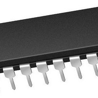
PIC16F1829-E/P Microchip Technology, PIC16F1829-E/P Datasheet - Page 219

PIC16F1829-E/P
Manufacturer Part Number
PIC16F1829-E/P
Description
14 KB Flash, 1K Bytes RAM, 32 MHz Int. Osc, 18 I/0, Enhanced Mid Range Core 20 P
Manufacturer
Microchip Technology
Series
PIC® XLP™ mTouch™ 16Fr
Datasheet
1.PIC16LF1829-ISO.pdf
(420 pages)
Specifications of PIC16F1829-E/P
Core Processor
PIC
Core Size
8-Bit
Speed
32MHz
Connectivity
I²C, LIN, SPI, UART/USART
Peripherals
Brown-out Detect/Reset, POR, PWM, WDT
Number Of I /o
17
Program Memory Size
14KB (8K x 14)
Program Memory Type
FLASH
Eeprom Size
256 x 8
Ram Size
1K x 8
Voltage - Supply (vcc/vdd)
1.8 V ~ 5.5 V
Data Converters
A/D 12x10b
Oscillator Type
Internal
Operating Temperature
-40°C ~ 125°C
Package / Case
*
Processor Series
PIC16F182x
Core
PIC
Data Bus Width
8 bit
Data Ram Size
1 KB
Interface Type
I2C, SPI, USART
Maximum Clock Frequency
32 MHz
Number Of Programmable I/os
18
Number Of Timers
5
Operating Supply Voltage
1.8 V to 5.5 V
Maximum Operating Temperature
+ 125 C
Mounting Style
Through Hole
Lead Free Status / RoHS Status
Lead free / RoHS Compliant
Lead Free Status / RoHS Status
Lead free / RoHS Compliant
- Current page: 219 of 420
- Download datasheet (5Mb)
24.2.5
The Compare mode is dependent upon the system
clock (F
down during Sleep mode, the Compare mode will not
function properly during Sleep.
TABLE 24-4:
2010 Microchip Technology Inc.
APFCON1
CCP1CON
CCP2CON
CCP3CON
CCP4CON
CCPRxL
CCPRxH
INLVLA
INLVLC
INTCON
PIE1
PIE2
PIE3
PIR1
PIR2
PIR3
T1CON
T1GCON
TMR1L
TMR1H
TRISA
TRISC
Legend:
Note
Name
1:
2:
3:
OSC
*
— = Unimplemented location, read as ‘0’. Shaded cells are not used by Compare mode.
Applies to ECCP modules only.
PIC16F/LF1829 only.
PIC16F/LF1825 only.
Page provides register information.
COMPARE DURING SLEEP
) for proper operation. Since F
Capture/Compare/PWM Register x Low Byte (LSB)
Capture/Compare/PWM Register x High Byte (MSB)
Holding Register for the Least Significant Byte of the 16-bit TMR1 Register
Holding Register for the Most Significant Byte of the 16-bit TMR1 Register
INLVLC7
TRISC7
TMR1GIE
TMR1GIF
TMR1GE
OSFIE
OSFIF
Bit 7
GIE
—
—
—
—
—
—
—
TMR1CS<1:0>
SUMMARY OF REGISTERS ASSOCIATED WITH COMPARE
P1M<1:0>
P2M<1:0>
(2)
(2)
INLVLC6
TRISC6
T1GPOL
(1)
(1)
PEIE
ADIE
C2IE
ADIF
Bit 6
C2IF
—
—
—
—
—
—
—
(2)
(2)
SDO2SEL
INLVLA5
INLVLC5
TMR0IE
CCP4IE
CCP4IF
TRISC5
T1GTM
TRISA5
RCIE
RCIF
Bit 5
C1IE
C1IF
T1CKPS<1:0>
DC1B<1:0>
DC2B<1:0>
DC3B<1:0>
DC4B<1:0>
OSC
(2)
SS2SEL
is shut
T1GSPM
INLVLA4
INLVLC4
CCP3IE
CCP3IF
TRISA4
TRISC4
INTE
EEIE
Bit 4
TXIE
TXIF
EEIF
Preliminary
(2)
T1GGO/DONE
T1OSCEN
P1DSEL
INLVLA3
INLVLC3
TMR6IE
SSP1IE
TMR6IF
TRISA3
TRISC3
BCL1IE
SSP1IF
BCL1IF
IOCIE
Bit 3
24.2.6
This module incorporates I/O pins that can be moved to
other locations with the use of the alternate pin function
registers, APFCON0 and APFCON1. To determine
which pins can be moved and what their default loca-
tions are upon a Reset, see
Pin Function”
PIC16F/LF1825/1829
INLVLA2
INLVLC2
T1SYNC
P1CSEL
T1GVAL
TMR0IF
CCP1IE
CCP1IF
TRISC2
TRISA2
ALTERNATE PIN LOCATIONS
Bit 2
CCP1M<3:0>
CCP2M<3:0>
CCP3M<3:0>
CCP4M<3:0>
—
—
—
—
for more information.
INLVLA1
INLVLC1
P2BSEL
TMR2IE
TMR4IE
TMR2IF
TMR4IF
TRISC1
TRISA1
Bit 1
INTF
—
—
—
T1GSS<1:0>
Section 12.1 “Alternate
CCP2SEL
TMR1ON
INLVLC0
INLVLA0
TMR1IE
CCP2IE
TMR1IF
CCP2IF
TRISA0
TRISC0
IOCIF
Bit 0
DS41440A-page 221
—
—
Register on
Page
218*
218*
205*
205*
126
240
240
240
240
131
142
100
199
200
129
140
93
94
95
96
98
99
Related parts for PIC16F1829-E/P
Image
Part Number
Description
Manufacturer
Datasheet
Request
R

Part Number:
Description:
IC, 8BIT MCU, PIC16F, 32MHZ, SOIC-18
Manufacturer:
Microchip Technology
Datasheet:

Part Number:
Description:
IC, 8BIT MCU, PIC16F, 32MHZ, SSOP-20
Manufacturer:
Microchip Technology
Datasheet:

Part Number:
Description:
IC, 8BIT MCU, PIC16F, 32MHZ, DIP-18
Manufacturer:
Microchip Technology
Datasheet:

Part Number:
Description:
IC, 8BIT MCU, PIC16F, 32MHZ, QFN-28
Manufacturer:
Microchip Technology
Datasheet:

Part Number:
Description:
IC, 8BIT MCU, PIC16F, 32MHZ, QFN-28
Manufacturer:
Microchip Technology
Datasheet:

Part Number:
Description:
IC, 8BIT MCU, PIC16F, 32MHZ, QFN-28
Manufacturer:
Microchip Technology
Datasheet:

Part Number:
Description:
IC, 8BIT MCU, PIC16F, 32MHZ, SSOP-20
Manufacturer:
Microchip Technology
Datasheet:

Part Number:
Description:
IC, 8BIT MCU, PIC16F, 20MHZ, DIP-40
Manufacturer:
Microchip Technology
Datasheet:

Part Number:
Description:
IC, 8BIT MCU, PIC16F, 32MHZ, QFN-28
Manufacturer:
Microchip Technology
Datasheet:

Part Number:
Description:
IC, 8BIT MCU, PIC16F, 20MHZ, MQFP-44
Manufacturer:
Microchip Technology
Datasheet:

Part Number:
Description:
IC, 8BIT MCU, PIC16F, 20MHZ, QFN-20
Manufacturer:
Microchip Technology
Datasheet:

Part Number:
Description:
IC, 8BIT MCU, PIC16F, 32MHZ, QFN-28
Manufacturer:
Microchip Technology
Datasheet:

Part Number:
Description:
MCU 14KB FLASH 768B RAM 64-TQFP
Manufacturer:
Microchip Technology
Datasheet:

Part Number:
Description:
7 KB Flash, 384 Bytes RAM, 32 MHz Int. Osc, 16 I/0, Enhanced Mid Range Core, Low
Manufacturer:
Microchip Technology

Part Number:
Description:
14KB Flash, 512B RAM, 256B EEPROM, LCD, 1.8-5.5V 40 UQFN 5x5x0.5mm TUBE
Manufacturer:
Microchip Technology
Datasheet:


