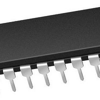
PIC16F1829-E/P Microchip Technology, PIC16F1829-E/P Datasheet - Page 224

PIC16F1829-E/P
Manufacturer Part Number
PIC16F1829-E/P
Description
14 KB Flash, 1K Bytes RAM, 32 MHz Int. Osc, 18 I/0, Enhanced Mid Range Core 20 P
Manufacturer
Microchip Technology
Series
PIC® XLP™ mTouch™ 16Fr
Datasheet
1.PIC16LF1829-ISO.pdf
(420 pages)
Specifications of PIC16F1829-E/P
Core Processor
PIC
Core Size
8-Bit
Speed
32MHz
Connectivity
I²C, LIN, SPI, UART/USART
Peripherals
Brown-out Detect/Reset, POR, PWM, WDT
Number Of I /o
17
Program Memory Size
14KB (8K x 14)
Program Memory Type
FLASH
Eeprom Size
256 x 8
Ram Size
1K x 8
Voltage - Supply (vcc/vdd)
1.8 V ~ 5.5 V
Data Converters
A/D 12x10b
Oscillator Type
Internal
Operating Temperature
-40°C ~ 125°C
Package / Case
*
Processor Series
PIC16F182x
Core
PIC
Data Bus Width
8 bit
Data Ram Size
1 KB
Interface Type
I2C, SPI, USART
Maximum Clock Frequency
32 MHz
Number Of Programmable I/os
18
Number Of Timers
5
Operating Supply Voltage
1.8 V to 5.5 V
Maximum Operating Temperature
+ 125 C
Mounting Style
Through Hole
Lead Free Status / RoHS Status
Lead free / RoHS Compliant
Lead Free Status / RoHS Status
Lead free / RoHS Compliant
- Current page: 224 of 420
- Download datasheet (5Mb)
PIC16F/LF1825/1829
24.4
The enhanced PWM function described in this section is
available for CCP modules ECCP1 and ECCP2, with
any differences between modules noted.
The enhanced PWM mode generates a Pulse-Width
Modulation (PWM) signal on up to four different output
pins with up to 10 bits of resolution. The period, duty
cycle, and resolution are controlled by the following
registers:
• PRx registers
• TxCON registers
• CCPRxL registers
• CCPxCON registers
The ECCP modules have the following additional PWM
registers which control Auto-shutdown, Auto-restart,
Dead-band Delay and PWM Steering modes:
• CCPxAS registers
• PSTRxCON registers
• PWMxCON registers
The enhanced PWM module can generate the following
five PWM Output modes:
• Single PWM
• Half-Bridge PWM
• Full-Bridge PWM, Forward Mode
• Full-Bridge PWM, Reverse Mode
• Single PWM with PWM Steering Mode
FIGURE 24-5:
DS41440A-page 226
Note 1:
CCPRxH (Slave)
Duty Cycle Registers
Comparator
PWM (Enhanced Mode)
CCPRxL
PRx
TMRx
Comparator
The 8-bit timer TMRx register is concatenated with the 2-bit internal Q clock, or 2 bits of the prescaler to create the 10-bit time
base.
(1)
EXAMPLE SIMPLIFIED BLOCK DIAGRAM OF THE ENHANCED PWM MODE
Clear Timer,
toggle PWM pin and
latch duty cycle
DCxB<1:0>
R
S
PxM<1:0>
Q
Preliminary
PWMxCON
Controller
Output
2
CCPx/PxA
PxB
PxC
PxD
To select an Enhanced PWM Output mode, the PxM bits
of the CCPxCON register must be configured
appropriately.
The PWM outputs are multiplexed with I/O pins and are
designated PxA, PxB, PxC and PxD. The polarity of the
PWM pins is configurable and is selected by setting the
CCPxM bits in the CCPxCON register appropriately.
Figure 24-5
diagram of the Enhanced PWM module.
Figure 24-8
Enhanced PWM modes.
4
CCPxM<3:0>
Note 1: The corresponding TRIS bit must be
2: Clearing the CCPxCON register will
3: Any pin not used in the enhanced PWM
4: To
TRISx
TRISx
TRISx
TRISx
cleared to enable the PWM output on the
CCPx pin.
relinquish control of the CCPx pin.
mode is available for alternate pin
functions, if applicable.
incomplete waveform when the PWM is
first enabled, the ECCP module waits
until the start of a new PWM period
before generating a PWM signal.
shows an example of a simplified block
shows the pin assignments for various
prevent
2010 Microchip Technology Inc.
the
CCPx/PxA
PxB
PxD
PxC
generation
of
an
Related parts for PIC16F1829-E/P
Image
Part Number
Description
Manufacturer
Datasheet
Request
R

Part Number:
Description:
IC, 8BIT MCU, PIC16F, 32MHZ, SOIC-18
Manufacturer:
Microchip Technology
Datasheet:

Part Number:
Description:
IC, 8BIT MCU, PIC16F, 32MHZ, SSOP-20
Manufacturer:
Microchip Technology
Datasheet:

Part Number:
Description:
IC, 8BIT MCU, PIC16F, 32MHZ, DIP-18
Manufacturer:
Microchip Technology
Datasheet:

Part Number:
Description:
IC, 8BIT MCU, PIC16F, 32MHZ, QFN-28
Manufacturer:
Microchip Technology
Datasheet:

Part Number:
Description:
IC, 8BIT MCU, PIC16F, 32MHZ, QFN-28
Manufacturer:
Microchip Technology
Datasheet:

Part Number:
Description:
IC, 8BIT MCU, PIC16F, 32MHZ, QFN-28
Manufacturer:
Microchip Technology
Datasheet:

Part Number:
Description:
IC, 8BIT MCU, PIC16F, 32MHZ, SSOP-20
Manufacturer:
Microchip Technology
Datasheet:

Part Number:
Description:
IC, 8BIT MCU, PIC16F, 20MHZ, DIP-40
Manufacturer:
Microchip Technology
Datasheet:

Part Number:
Description:
IC, 8BIT MCU, PIC16F, 32MHZ, QFN-28
Manufacturer:
Microchip Technology
Datasheet:

Part Number:
Description:
IC, 8BIT MCU, PIC16F, 20MHZ, MQFP-44
Manufacturer:
Microchip Technology
Datasheet:

Part Number:
Description:
IC, 8BIT MCU, PIC16F, 20MHZ, QFN-20
Manufacturer:
Microchip Technology
Datasheet:

Part Number:
Description:
IC, 8BIT MCU, PIC16F, 32MHZ, QFN-28
Manufacturer:
Microchip Technology
Datasheet:

Part Number:
Description:
MCU 14KB FLASH 768B RAM 64-TQFP
Manufacturer:
Microchip Technology
Datasheet:

Part Number:
Description:
7 KB Flash, 384 Bytes RAM, 32 MHz Int. Osc, 16 I/0, Enhanced Mid Range Core, Low
Manufacturer:
Microchip Technology

Part Number:
Description:
14KB Flash, 512B RAM, 256B EEPROM, LCD, 1.8-5.5V 40 UQFN 5x5x0.5mm TUBE
Manufacturer:
Microchip Technology
Datasheet:


