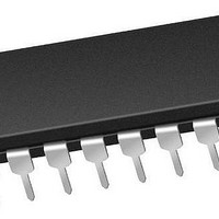
PIC16F1829-E/P Microchip Technology, PIC16F1829-E/P Datasheet - Page 247

PIC16F1829-E/P
Manufacturer Part Number
PIC16F1829-E/P
Description
14 KB Flash, 1K Bytes RAM, 32 MHz Int. Osc, 18 I/0, Enhanced Mid Range Core 20 P
Manufacturer
Microchip Technology
Series
PIC® XLP™ mTouch™ 16Fr
Datasheet
1.PIC16LF1829-ISO.pdf
(420 pages)
Specifications of PIC16F1829-E/P
Core Processor
PIC
Core Size
8-Bit
Speed
32MHz
Connectivity
I²C, LIN, SPI, UART/USART
Peripherals
Brown-out Detect/Reset, POR, PWM, WDT
Number Of I /o
17
Program Memory Size
14KB (8K x 14)
Program Memory Type
FLASH
Eeprom Size
256 x 8
Ram Size
1K x 8
Voltage - Supply (vcc/vdd)
1.8 V ~ 5.5 V
Data Converters
A/D 12x10b
Oscillator Type
Internal
Operating Temperature
-40°C ~ 125°C
Package / Case
*
Processor Series
PIC16F182x
Core
PIC
Data Bus Width
8 bit
Data Ram Size
1 KB
Interface Type
I2C, SPI, USART
Maximum Clock Frequency
32 MHz
Number Of Programmable I/os
18
Number Of Timers
5
Operating Supply Voltage
1.8 V to 5.5 V
Maximum Operating Temperature
+ 125 C
Mounting Style
Through Hole
Lead Free Status / RoHS Status
Lead free / RoHS Compliant
Lead Free Status / RoHS Status
Lead free / RoHS Compliant
- Current page: 247 of 420
- Download datasheet (5Mb)
FIGURE 25-4:
25.2.1
The MSSPx module has five registers for SPI mode
operation. These are:
• MSSPx STATUS register (SSPxSTAT)
• MSSPx Control Register 1 (SSPxCON1)
• MSSPx Control Register 3 (SSPxCON3)
• MSSPx Data Buffer register (SSPxBUF)
• MSSPx Address register (SSPxADD)
• MSSPx Shift register (SSPxSR)
SSPxCON1 and SSPxSTAT are the control and
STATUS registers in SPI mode operation. The
SSPxCON1 register is readable and writable. The
lower 6 bits of the SSPxSTAT are read-only. The upper
two bits of the SSPxSTAT are read/write.
In one SPI master mode, SSPxADD can be loaded
with a value used in the Baud Rate Generator. More
information on the Baud Rate Generator is available in
Section 25.7 “Baud Rate
SSPxSR is the shift register used for shifting data in
and out. SSPxBUF provides indirect access to the
SSPxSR register. SSPxBUF is the buffer register to
which data bytes are written, and from which data
bytes are read.
In receive operations, SSPxSR and SSPxBUF
together create a buffered receiver. When SSPxSR
receives a complete byte, it is transferred to SSPxBUF
and the SSPxIF interrupt is set.
During transmission, the SSPxBUF is not buffered. A
write to SSPxBUF will write to both SSPxBUF and
SSPxSR.
2010 Microchip Technology Inc.
(Not directly accessible)
SPI MODE REGISTERS
SPI Master
SPI MASTER AND MULTIPLE SLAVE CONNECTION
Generator”.
General I/O
General I/O
General I/O
SDOx
SCKx
SDIx
Preliminary
PIC16F/LF1825/1829
SCKx
SDIx
SDOx
SSx
SCKx
SDIx
SDOx
SSx
SCKx
SDIx
SDOx
SSx
SPI Slave
SPI Slave
SPI Slave
#1
#2
#3
DS41440A-page 249
Related parts for PIC16F1829-E/P
Image
Part Number
Description
Manufacturer
Datasheet
Request
R

Part Number:
Description:
IC, 8BIT MCU, PIC16F, 32MHZ, SOIC-18
Manufacturer:
Microchip Technology
Datasheet:

Part Number:
Description:
IC, 8BIT MCU, PIC16F, 32MHZ, SSOP-20
Manufacturer:
Microchip Technology
Datasheet:

Part Number:
Description:
IC, 8BIT MCU, PIC16F, 32MHZ, DIP-18
Manufacturer:
Microchip Technology
Datasheet:

Part Number:
Description:
IC, 8BIT MCU, PIC16F, 32MHZ, QFN-28
Manufacturer:
Microchip Technology
Datasheet:

Part Number:
Description:
IC, 8BIT MCU, PIC16F, 32MHZ, QFN-28
Manufacturer:
Microchip Technology
Datasheet:

Part Number:
Description:
IC, 8BIT MCU, PIC16F, 32MHZ, QFN-28
Manufacturer:
Microchip Technology
Datasheet:

Part Number:
Description:
IC, 8BIT MCU, PIC16F, 32MHZ, SSOP-20
Manufacturer:
Microchip Technology
Datasheet:

Part Number:
Description:
IC, 8BIT MCU, PIC16F, 20MHZ, DIP-40
Manufacturer:
Microchip Technology
Datasheet:

Part Number:
Description:
IC, 8BIT MCU, PIC16F, 32MHZ, QFN-28
Manufacturer:
Microchip Technology
Datasheet:

Part Number:
Description:
IC, 8BIT MCU, PIC16F, 20MHZ, MQFP-44
Manufacturer:
Microchip Technology
Datasheet:

Part Number:
Description:
IC, 8BIT MCU, PIC16F, 20MHZ, QFN-20
Manufacturer:
Microchip Technology
Datasheet:

Part Number:
Description:
IC, 8BIT MCU, PIC16F, 32MHZ, QFN-28
Manufacturer:
Microchip Technology
Datasheet:

Part Number:
Description:
MCU 14KB FLASH 768B RAM 64-TQFP
Manufacturer:
Microchip Technology
Datasheet:

Part Number:
Description:
7 KB Flash, 384 Bytes RAM, 32 MHz Int. Osc, 16 I/0, Enhanced Mid Range Core, Low
Manufacturer:
Microchip Technology

Part Number:
Description:
14KB Flash, 512B RAM, 256B EEPROM, LCD, 1.8-5.5V 40 UQFN 5x5x0.5mm TUBE
Manufacturer:
Microchip Technology
Datasheet:


