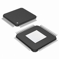
PIC24FJ256DA210T-I/BG Microchip Technology, PIC24FJ256DA210T-I/BG Datasheet - Page 148

PIC24FJ256DA210T-I/BG
Manufacturer Part Number
PIC24FJ256DA210T-I/BG
Description
16-bit, 256KB Flash, 96K RAM, USB, Graphics 121 XBGA 10x10x1.20mm T/R
Manufacturer
Microchip Technology
Series
PIC® 24Fr
Specifications of PIC24FJ256DA210T-I/BG
Core Processor
PIC
Core Size
16-Bit
Speed
32MHz
Connectivity
I²C, IrDA, SPI, UART/USART, USB OTG
Peripherals
Brown-out Detect/Reset, GFX, LVD, POR, PWM, WDT
Number Of I /o
84
Program Memory Size
256KB (85.5K x 24)
Program Memory Type
FLASH
Ram Size
96K x 8
Voltage - Supply (vcc/vdd)
2.2 V ~ 3.6 V
Data Converters
A/D 24x10b
Oscillator Type
Internal
Operating Temperature
-40°C ~ 85°C
Package / Case
121-TFBGA
Lead Free Status / RoHS Status
Lead free / RoHS Compliant
Eeprom Size
-
Lead Free Status / RoHS Status
Lead free / RoHS Compliant
Available stocks
Company
Part Number
Manufacturer
Quantity
Price
Company:
Part Number:
PIC24FJ256DA210T-I/BG
Manufacturer:
Microchip Technology
Quantity:
10 000
- Current page: 148 of 408
- Download datasheet (4Mb)
PIC24FJ256DA210 FAMILY
8.4
With few limitations, applications are free to switch
between any of the four clock sources (POSC, SOSC,
FRC and LPRC) under software control and at any
time. To limit the possible side effects that could result
from this flexibility, PIC24F devices have a safeguard
lock built into the switching process.
8.4.1
To enable clock switching, the FCKSM1 Configuration
bit in CW2 must be programmed to ‘0’. (Refer to
Section 27.1 “Configuration Bits” for further details.)
If the FCKSM1 Configuration bit is unprogrammed (‘1’),
the clock switching function and Fail-Safe Clock Monitor
function are disabled. This is the default setting.
The NOSCx (OSCCON<10:8>) control bits do not
control the clock selection when clock switching is
disabled. However, the COSCx (OSCCON<14:12>)
control bits will reflect the clock source selected by the
FNOSCx Configuration bits.
The OSWEN (OSCCON<0>) control bit has no effect
when clock switching is disabled; It is held at ‘0’ at all
times.
8.4.2
At a minimum, performing a clock switch requires this
basic sequence:
1.
2.
3.
4.
5.
DS39969B-page 148
Note:
If desired, read the COSCx (OSCCON<14:12>)
control bits to determine the current oscillator
source.
Perform the unlock sequence to allow a write to
the OSCCON register high byte.
Write the appropriate value to the NOSCx
(OSCCON<10:8>) control bits for the new
oscillator source.
Perform the unlock sequence to allow a write to
the OSCCON register low byte.
Set the OSWEN bit to initiate the oscillator
switch.
Clock Switching Operation
The Primary Oscillator mode has three
different submodes (XT, HS and EC)
which are determined by the POSCMDx
Configuration bits. While an application
can switch to and from Primary Oscillator
mode in software, it cannot switch
between the different primary submodes
without reprogramming the device.
ENABLING CLOCK SWITCHING
OSCILLATOR SWITCHING
SEQUENCE
Once the basic sequence is completed, the system
clock hardware responds automatically as follows:
1.
2.
3.
4.
5.
6.
Note 1: The processor will continue to execute
The clock switching hardware compares the
COSCx bits with the new value of the NOSCx
bits. If they are the same, then the clock switch
is a redundant operation. In this case, the
OSWEN bit is cleared automatically and the
clock switch is aborted.
If a valid clock switch has been initiated, the
LOCK (OSCCON<5>) and CF (OSCCON<3>)
bits are cleared.
The new oscillator is turned on by the hardware
if it is not currently running. If a crystal oscillator
must be turned on, the hardware will wait until
the OST expires. If the new source is using the
PLL, then the hardware waits until a PLL lock is
detected (LOCK = 1).
The hardware waits for 10 clock cycles from the
new clock source and then performs the clock
switch.
The hardware clears the OSWEN bit to indicate a
successful clock transition. In addition, the
NOSCx bit values are transferred to the COSCx
bits.
The old clock source is turned off at this time,
with the exception of LPRC (if WDT or FSCM
are enabled) or SOSC (if SOSCEN remains
set).
2: Direct clock switches between any
code throughout the clock switching
sequence. Timing-sensitive code should
not be executed during this time.
Primary Oscillator mode with PLL and
FRCPLL modes are not permitted. This
applies to clock switches in either direc-
tion. In these instances, the application
must switch to FRC mode as a transition
clock source between the two PLL
modes.
2010 Microchip Technology Inc.
Related parts for PIC24FJ256DA210T-I/BG
Image
Part Number
Description
Manufacturer
Datasheet
Request
R

Part Number:
Description:
Manufacturer:
Microchip Technology Inc.
Datasheet:

Part Number:
Description:
Manufacturer:
Microchip Technology Inc.
Datasheet:

Part Number:
Description:
Manufacturer:
Microchip Technology Inc.
Datasheet:

Part Number:
Description:
Manufacturer:
Microchip Technology Inc.
Datasheet:

Part Number:
Description:
Manufacturer:
Microchip Technology Inc.
Datasheet:

Part Number:
Description:
Manufacturer:
Microchip Technology Inc.
Datasheet:

Part Number:
Description:
Manufacturer:
Microchip Technology Inc.
Datasheet:

Part Number:
Description:
Manufacturer:
Microchip Technology Inc.
Datasheet:


