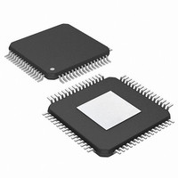
PIC24FJ256DA210T-I/BG Microchip Technology, PIC24FJ256DA210T-I/BG Datasheet - Page 149

PIC24FJ256DA210T-I/BG
Manufacturer Part Number
PIC24FJ256DA210T-I/BG
Description
16-bit, 256KB Flash, 96K RAM, USB, Graphics 121 XBGA 10x10x1.20mm T/R
Manufacturer
Microchip Technology
Series
PIC® 24Fr
Specifications of PIC24FJ256DA210T-I/BG
Core Processor
PIC
Core Size
16-Bit
Speed
32MHz
Connectivity
I²C, IrDA, SPI, UART/USART, USB OTG
Peripherals
Brown-out Detect/Reset, GFX, LVD, POR, PWM, WDT
Number Of I /o
84
Program Memory Size
256KB (85.5K x 24)
Program Memory Type
FLASH
Ram Size
96K x 8
Voltage - Supply (vcc/vdd)
2.2 V ~ 3.6 V
Data Converters
A/D 24x10b
Oscillator Type
Internal
Operating Temperature
-40°C ~ 85°C
Package / Case
121-TFBGA
Lead Free Status / RoHS Status
Lead free / RoHS Compliant
Eeprom Size
-
Lead Free Status / RoHS Status
Lead free / RoHS Compliant
Available stocks
Company
Part Number
Manufacturer
Quantity
Price
Company:
Part Number:
PIC24FJ256DA210T-I/BG
Manufacturer:
Microchip Technology
Quantity:
10 000
- Current page: 149 of 408
- Download datasheet (4Mb)
A recommended code sequence for a clock switch
includes the following:
1.
2.
3.
4.
5.
6.
7.
8.
The core sequence for unlocking the OSCCON register
and initiating a clock switch is shown in Example 8-1.
EXAMPLE 8-1:
2010 Microchip Technology Inc.
;Place the new oscillator selection in W0
;OSCCONH (high byte) Unlock Sequence
MOV
MOV
MOV
MOV.b
MOV.b
;Set new oscillator selection
MOV.b
;OSCCONL (low byte) unlock sequence
MOV
MOV
MOV
MOV.b
MOV.b
;Start oscillator switch operation
BSET
Disable interrupts during the OSCCON register
unlock and write sequence.
Execute the unlock sequence for the OSCCON
high byte by writing 78h
OSCCON<15:8>
instructions.
Write new oscillator source to the NOSCx bits in
the instruction immediately following the unlock
sequence.
Execute the unlock sequence for the OSCCON
low
OSCCON<7:0> in two back-to-back instructions.
Set the OSWEN bit in the instruction immediately
following the unlock sequence.
Continue
clock-sensitive (optional).
Invoke an appropriate amount of software delay
(cycle counting) to allow the selected oscillator
and/or PLL to start and stabilize.
Check to see if OSWEN is ‘0’. If it is, the switch
was successful. If OSWEN is still set, then
check the LOCK bit to determine the cause of
failure.
byte
#OSCCONH, w1
#0x78, w2
#0x9A, w3
w2, [w1]
w3, [w1]
WREG, OSCCONH
#OSCCONL, w1
#0x46, w2
#0x57, w3
w2, [w1]
w3, [w1]
OSCCON,#0
to
by
execute
writing
BASIC CODE SEQUENCE
FOR CLOCK SWITCHING
IN ASSEMBLY
in
code
46h
two
and 9Ah to
and
that
back-to-back
57h
is
PIC24FJ256DA210 FAMILY
not
to
8.5
The 96 MHz PLL block is implemented to generate the
stable 48 MHz clock required for full-speed USB
operation, a programmable clock output for the
graphics controller module and the system clock from
the same oscillator source. The 96 MHz PLL block is
shown in Figure 8-2.
The 96 MHz PLL block requires a 4 MHz input signal; it
uses this to generate a 96 MHz signal from a fixed, 24x
PLL. This is, in turn, divided into three branches. The first
branch generates the USB clock, the second branch
generates the system clock and the third branch gener-
ates the graphics clock. The 96 MHz PLL block can be
enabled and disabled using the PLL96MHZ Configura-
tion bit (Configuration Word<11>) or through the PLLEN
(CLKDIV<5>)
Configuration bit is not set. Note that the PLL96MHZ
Configuration bit and PLLEN register bit are available
only for PIC24F devices with USB and graphics
controller modules.
The 96 MHz PLL prescaler does not automatically
sense the incoming oscillator frequency. The user must
manually configure the PLL divider to generate the
required 4 MHz output, using the PLLDIV<2:0> Config-
uration bits (Configuration Word 2<14:12> in most
devices).
96 MHz PLL Block
control
bit
when
DS39969B-page 149
the
PLL96MHZ
Related parts for PIC24FJ256DA210T-I/BG
Image
Part Number
Description
Manufacturer
Datasheet
Request
R

Part Number:
Description:
Manufacturer:
Microchip Technology Inc.
Datasheet:

Part Number:
Description:
Manufacturer:
Microchip Technology Inc.
Datasheet:

Part Number:
Description:
Manufacturer:
Microchip Technology Inc.
Datasheet:

Part Number:
Description:
Manufacturer:
Microchip Technology Inc.
Datasheet:

Part Number:
Description:
Manufacturer:
Microchip Technology Inc.
Datasheet:

Part Number:
Description:
Manufacturer:
Microchip Technology Inc.
Datasheet:

Part Number:
Description:
Manufacturer:
Microchip Technology Inc.
Datasheet:

Part Number:
Description:
Manufacturer:
Microchip Technology Inc.
Datasheet:


