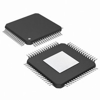
PIC24FJ256DA210T-I/BG Microchip Technology, PIC24FJ256DA210T-I/BG Datasheet - Page 151

PIC24FJ256DA210T-I/BG
Manufacturer Part Number
PIC24FJ256DA210T-I/BG
Description
16-bit, 256KB Flash, 96K RAM, USB, Graphics 121 XBGA 10x10x1.20mm T/R
Manufacturer
Microchip Technology
Series
PIC® 24Fr
Specifications of PIC24FJ256DA210T-I/BG
Core Processor
PIC
Core Size
16-Bit
Speed
32MHz
Connectivity
I²C, IrDA, SPI, UART/USART, USB OTG
Peripherals
Brown-out Detect/Reset, GFX, LVD, POR, PWM, WDT
Number Of I /o
84
Program Memory Size
256KB (85.5K x 24)
Program Memory Type
FLASH
Ram Size
96K x 8
Voltage - Supply (vcc/vdd)
2.2 V ~ 3.6 V
Data Converters
A/D 24x10b
Oscillator Type
Internal
Operating Temperature
-40°C ~ 85°C
Package / Case
121-TFBGA
Lead Free Status / RoHS Status
Lead free / RoHS Compliant
Eeprom Size
-
Lead Free Status / RoHS Status
Lead free / RoHS Compliant
Available stocks
Company
Part Number
Manufacturer
Quantity
Price
Company:
Part Number:
PIC24FJ256DA210T-I/BG
Manufacturer:
Microchip Technology
Quantity:
10 000
- Current page: 151 of 408
- Download datasheet (4Mb)
8.5.2
In the USB-On-The-Go module in PIC24FJ256DA210
family of devices, the primary oscillator with the PLL
block can be used as a valid clock source for USB oper-
ation. The FRC oscillator (implemented with ±0.25%
accuracy) can be combined with a PLL block, providing
another option for a valid USB clock source. There is
no provision to provide a separate external 48 MHz
clock to the USB module. The USB module sources its
TABLE 8-3:
8.5.3
When
PIC24FJ256DA210 family devices, users must always
observe these rules in configuring the system clock:
• For USB operation, the selected clock source
• The Primary Oscillator/PLL modes are the only
• While the FRCPLL Oscillator mode is used for
All other oscillator modes are available; however, USB
operation is not possible when these modes are
selected. They may still be useful in cases where other
power levels of operation are desirable and the USB
module is not needed (e.g., the application is sleeping
and waiting for a bus attachment).
2010 Microchip Technology Inc.
Note:
(EC, HS or XT) must meet the USB clock
tolerance requirements.
oscillator configurations that permit USB opera-
tion. There is no provision to provide a separate
external clock source to the USB module.
USB applications, users must always ensure that
the FRC source is configured to provide a
frequency of 4 MHz or 8 MHz (RCDIV<2:0> = 001
or 000) and that the USB PLL prescaler is
configured appropriately.
Input Oscillator Frequency
using
For USB devices, the use of a primary oscillator or external clock source, with a frequency above 32 MHz,
does not imply that the device’s system clock can be run at the same speed when the USB module is not
used. The maximum system clock for all PIC24F devices is 32 MHz.
USB CLOCK GENERATION
CONSIDERATIONS FOR USB
OPERATION
48 MHz
32 MHz
24 MHz
20 MHz
16 MHz
12 MHz
8 MHz
4 MHz
the
VALID OSCILLATOR CONFIGURATIONS FOR USB OPERATIONS
USB
On-The-Go
ECPLL, HSPLL, XTPLL, FRCPLL
ECPLL, HSPLL, XTPLL, FRCPLL
module
PIC24FJ256DA210 FAMILY
HSPLL, ECPLL
HSPLL, ECPLL
HSPLL, ECPLL
HSPLL, ECPLL
HSPLL, ECPLL
Clock Mode
in
ECPLL
clock signal from 96 MHz PLL. Due to the requirement
that a 4 MHz input must be provided to generate the
96 MHz signal, the oscillator operation is limited to a
range of possible values. Table 8-3 shows the valid
oscillator configurations (i.e., ECPLL, HSPLL, XTPLL
and FRCPLL) for USB operation. This sets the correct
PLLDIV configuration for the specified oscillator
frequency and the output frequency of the USB clock
branch is always 48 MHz.
8.5.4
Two stable clock signals are generated for the graphics
controller in the PIC24FJ256DA210 family of devices.
The first clock is for the graphics controller module logic
and the second clock is for the display module interface
logic that generates the signals for the display glass.
Figure 8-2 shows this logic in the graphics clock
sub-block. Both clock signals are generated either from
the Graphics Clock Option 1 (96 MHz branch) or the
Graphics Clock Option 2 (48 MHz branch). Selection is
set
(CLKDIV<4>) control bit. Graphics controller module
logic directly uses the output of that multiplexer while
the display module interface clock is further condi-
tioned through a postscaler to generate 128 possible
frequencies. The final clock output signal is selected
through a multiplexer using the GCLKDIV<6:0>
(CLKDIV2<15:9>) control bits. The 128 selections vary
in increments of 0.25, 0.5, and 1.0. Refer to Table 8-4
for details. Note that for applications that use the
graphics controller (GFX) module, the 96 MHz PLL
must be enabled.
in
the
GRAPHICS CLOCK GENERATION
multiplexer
(PLLDIV<2:0>)
PLL Division
12 (111)
using
8 (110)
6 (101)
5 (100)
4 (011)
3 (010)
2 (001)
1 (000)
DS39969B-page 151
the
G1CLKSEL
Related parts for PIC24FJ256DA210T-I/BG
Image
Part Number
Description
Manufacturer
Datasheet
Request
R

Part Number:
Description:
Manufacturer:
Microchip Technology Inc.
Datasheet:

Part Number:
Description:
Manufacturer:
Microchip Technology Inc.
Datasheet:

Part Number:
Description:
Manufacturer:
Microchip Technology Inc.
Datasheet:

Part Number:
Description:
Manufacturer:
Microchip Technology Inc.
Datasheet:

Part Number:
Description:
Manufacturer:
Microchip Technology Inc.
Datasheet:

Part Number:
Description:
Manufacturer:
Microchip Technology Inc.
Datasheet:

Part Number:
Description:
Manufacturer:
Microchip Technology Inc.
Datasheet:

Part Number:
Description:
Manufacturer:
Microchip Technology Inc.
Datasheet:


