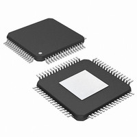
PIC24FJ256DA210T-I/BG Microchip Technology, PIC24FJ256DA210T-I/BG Datasheet - Page 166

PIC24FJ256DA210T-I/BG
Manufacturer Part Number
PIC24FJ256DA210T-I/BG
Description
16-bit, 256KB Flash, 96K RAM, USB, Graphics 121 XBGA 10x10x1.20mm T/R
Manufacturer
Microchip Technology
Series
PIC® 24Fr
Specifications of PIC24FJ256DA210T-I/BG
Core Processor
PIC
Core Size
16-Bit
Speed
32MHz
Connectivity
I²C, IrDA, SPI, UART/USART, USB OTG
Peripherals
Brown-out Detect/Reset, GFX, LVD, POR, PWM, WDT
Number Of I /o
84
Program Memory Size
256KB (85.5K x 24)
Program Memory Type
FLASH
Ram Size
96K x 8
Voltage - Supply (vcc/vdd)
2.2 V ~ 3.6 V
Data Converters
A/D 24x10b
Oscillator Type
Internal
Operating Temperature
-40°C ~ 85°C
Package / Case
121-TFBGA
Lead Free Status / RoHS Status
Lead free / RoHS Compliant
Eeprom Size
-
Lead Free Status / RoHS Status
Lead free / RoHS Compliant
Available stocks
Company
Part Number
Manufacturer
Quantity
Price
Company:
Part Number:
PIC24FJ256DA210T-I/BG
Manufacturer:
Microchip Technology
Quantity:
10 000
- Current page: 166 of 408
- Download datasheet (4Mb)
PIC24FJ256DA210 FAMILY
10.4.3.2
In contrast to inputs, the outputs of the Peripheral Pin
Select options are mapped on the basis of the pin. In
this case, a control register associated with a particular
pin dictates the peripheral output to be mapped. The
RPORx registers are used to control output mapping.
Each register contains two 6-bit fields, with each field
being associated with one RPn pin (see Register 10-29
through Register 10-44). The value of the bit field
TABLE 10-4:
DS39969B-page 166
Note 1:
Output Function Number
2:
3:
Setting the RPORx register with the listed value assigns that output function to the associated RPn pin.
The NULL function is assigned to all RPn outputs at device Reset and disables the RPn output function.
IrDA
Output Mapping
®
37-63
SELECTABLE OUTPUT SOURCES (MAPS FUNCTION TO OUTPUT)
BCLK functionality uses this output.
10
11
12
18
19
20
21
22
23
24
25
28
29
30
31
32
33
34
35
36
0
1
2
3
4
5
6
7
8
9
(1)
SCK1OUT
SCK2OUT
SCK3OUT
Function
U1RTS
U2RTS
U3RTS
U4RTS
SS1OUT
SS2OUT
SS3OUT
(unused)
NULL
C1OUT
C2OUT
C3OUT
SDO1
SDO2
SDO3
U1TX
U2TX
U3TX
U4TX
OC1
OC2
OC3
OC4
OC5
OC6
OC7
OC8
OC9
(2)
(3)
(3)
(3)
(3)
corresponds to one of the peripherals and that
peripheral’s output is mapped to the pin (see
Table 10-4).
Because of the mapping technique, the list of peripher-
als for output mapping also includes a null value of
‘000000’. This permits any given pin to remain discon-
nected from the output of any of the pin-selectable
peripherals.
SPI1 Slave Select Output
SPI2 Slave Select Output
SPI3 Slave Select Output
UART1 Request To Send
UART2 Request To Send
UART4 Request To Send
UART3 Request To Send
2010 Microchip Technology Inc.
Comparator 1 Output
Comparator 2 Output
Comparator 3 Output
SPI1 Clock Output
SPI2 Clock Output
Output Compare 1
Output Compare 2
Output Compare 3
Output Compare 4
Output Compare 5
Output Compare 6
Output Compare 7
Output Compare 8
SPI3 Clock Output
Output Compare 9
SPI1 Data Output
SPI2 Data Output
SPI3 Data Output
UART1 Transmit
UART2 Transmit
UART3 Transmit
UART4 Transmit
Output Name
Null
NC
Related parts for PIC24FJ256DA210T-I/BG
Image
Part Number
Description
Manufacturer
Datasheet
Request
R

Part Number:
Description:
Manufacturer:
Microchip Technology Inc.
Datasheet:

Part Number:
Description:
Manufacturer:
Microchip Technology Inc.
Datasheet:

Part Number:
Description:
Manufacturer:
Microchip Technology Inc.
Datasheet:

Part Number:
Description:
Manufacturer:
Microchip Technology Inc.
Datasheet:

Part Number:
Description:
Manufacturer:
Microchip Technology Inc.
Datasheet:

Part Number:
Description:
Manufacturer:
Microchip Technology Inc.
Datasheet:

Part Number:
Description:
Manufacturer:
Microchip Technology Inc.
Datasheet:

Part Number:
Description:
Manufacturer:
Microchip Technology Inc.
Datasheet:


