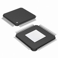
PIC24FJ256DA210T-I/BG Microchip Technology, PIC24FJ256DA210T-I/BG Datasheet - Page 234

PIC24FJ256DA210T-I/BG
Manufacturer Part Number
PIC24FJ256DA210T-I/BG
Description
16-bit, 256KB Flash, 96K RAM, USB, Graphics 121 XBGA 10x10x1.20mm T/R
Manufacturer
Microchip Technology
Series
PIC® 24Fr
Specifications of PIC24FJ256DA210T-I/BG
Core Processor
PIC
Core Size
16-Bit
Speed
32MHz
Connectivity
I²C, IrDA, SPI, UART/USART, USB OTG
Peripherals
Brown-out Detect/Reset, GFX, LVD, POR, PWM, WDT
Number Of I /o
84
Program Memory Size
256KB (85.5K x 24)
Program Memory Type
FLASH
Ram Size
96K x 8
Voltage - Supply (vcc/vdd)
2.2 V ~ 3.6 V
Data Converters
A/D 24x10b
Oscillator Type
Internal
Operating Temperature
-40°C ~ 85°C
Package / Case
121-TFBGA
Lead Free Status / RoHS Status
Lead free / RoHS Compliant
Eeprom Size
-
Lead Free Status / RoHS Status
Lead free / RoHS Compliant
Available stocks
Company
Part Number
Manufacturer
Quantity
Price
Company:
Part Number:
PIC24FJ256DA210T-I/BG
Manufacturer:
Microchip Technology
Quantity:
10 000
- Current page: 234 of 408
- Download datasheet (4Mb)
PIC24FJ256DA210 FAMILY
REGISTER 17-1:
DS39969B-page 234
bit 15
bit 7
Legend:
R = Readable bit
-n = Value at POR
bit 15
bit 14
bit 13
bit 12
bit 11
bit 10
bit 9-8
bit 7
bit 6
bit 5
Note 1:
UARTEN
R/W-0, HC
R/W-0
WAKE
2:
(1)
If UARTEN = 1, the peripheral inputs and outputs must be configured to an available RPn/RPIn pin. See
Section 10.4 “Peripheral Pin Select (PPS)” for more information.
This feature is only available for the 16x BRG mode (BRGH = 0).
UARTEN: UARTx Enable bit
1 = UARTx is enabled; all UARTx pins are controlled by UARTx as defined by UEN<1:0>
0 = UARTx is disabled; all UARTx pins are controlled by port latches; UARTx power consumption is minimal
Unimplemented: Read as ‘0’
USIDL: Stop in Idle Mode bit
1 = Discontinue module operation when device enters Idle mode
0 = Continue module operation in Idle mode
IREN: IrDA
1 = IrDA encoder and decoder are enabled
0 = IrDA encoder and decoder are disabled
RTSMD: Mode Selection for UxRTS Pin bit
1 = UxRTS pin is in Simplex mode
0 = UxRTS pin is in Flow Control mode
Unimplemented: Read as ‘0’
UEN<1:0>: UARTx Enable bits
11 = UxTX, UxRX and BCLKx pins are enabled and used; UxCTS pin is controlled by port latches
10 = UxTX, UxRX, UxCTS and UxRTS pins are enabled and used
01 = UxTX, UxRX and UxRTS pins are enabled and used; UxCTS pin is controlled by port latches
00 = UxTX and UxRX pins are enabled and used; UxCTS and UxRTS/BCLKx pins are controlled by port
WAKE: Wake-up on Start Bit Detect During Sleep Mode Enable bit
1 = UARTx will continue to sample the UxRX pin; interrupt is generated on the falling edge, bit is cleared
0 = No wake-up is enabled
LPBACK: UARTx Loopback Mode Select bit
1 = Enable Loopback mode
0 = Loopback mode is disabled
ABAUD: Auto-Baud Enable bit
1 = Enable baud rate measurement on the next character – requires reception of a Sync field (55h);
0 = Baud rate measurement is disabled or completed
LPBACK
R/W-0
in hardware on the following rising edge
cleared in hardware upon completion
U-0
—
latches
UxMODE: UARTx MODE REGISTER
®
Encoder and Decoder Enable bit
HC = Hardware Clearable bit
W = Writable bit
‘1’ = Bit is set
R/W-0, HC
ABAUD
USIDL
R/W-0
(1)
IREN
RXINV
R/W-0
R/W-0
(2)
U = Unimplemented bit, read as ‘0’
‘0’ = Bit is cleared
(2)
RTSMD
R/W-0
R/W-0
BRGH
PDSEL1
R/W-0
U-0
—
2010 Microchip Technology Inc.
x = Bit is unknown
PDSEL0
R/W-0
UEN1
R/W-0
STSEL
R/W-0
R/W-0
UEN0
bit 8
bit 0
Related parts for PIC24FJ256DA210T-I/BG
Image
Part Number
Description
Manufacturer
Datasheet
Request
R

Part Number:
Description:
Manufacturer:
Microchip Technology Inc.
Datasheet:

Part Number:
Description:
Manufacturer:
Microchip Technology Inc.
Datasheet:

Part Number:
Description:
Manufacturer:
Microchip Technology Inc.
Datasheet:

Part Number:
Description:
Manufacturer:
Microchip Technology Inc.
Datasheet:

Part Number:
Description:
Manufacturer:
Microchip Technology Inc.
Datasheet:

Part Number:
Description:
Manufacturer:
Microchip Technology Inc.
Datasheet:

Part Number:
Description:
Manufacturer:
Microchip Technology Inc.
Datasheet:

Part Number:
Description:
Manufacturer:
Microchip Technology Inc.
Datasheet:


