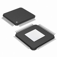
PIC24FJ256DA210T-I/BG Microchip Technology, PIC24FJ256DA210T-I/BG Datasheet - Page 281

PIC24FJ256DA210T-I/BG
Manufacturer Part Number
PIC24FJ256DA210T-I/BG
Description
16-bit, 256KB Flash, 96K RAM, USB, Graphics 121 XBGA 10x10x1.20mm T/R
Manufacturer
Microchip Technology
Series
PIC® 24Fr
Specifications of PIC24FJ256DA210T-I/BG
Core Processor
PIC
Core Size
16-Bit
Speed
32MHz
Connectivity
I²C, IrDA, SPI, UART/USART, USB OTG
Peripherals
Brown-out Detect/Reset, GFX, LVD, POR, PWM, WDT
Number Of I /o
84
Program Memory Size
256KB (85.5K x 24)
Program Memory Type
FLASH
Ram Size
96K x 8
Voltage - Supply (vcc/vdd)
2.2 V ~ 3.6 V
Data Converters
A/D 24x10b
Oscillator Type
Internal
Operating Temperature
-40°C ~ 85°C
Package / Case
121-TFBGA
Lead Free Status / RoHS Status
Lead free / RoHS Compliant
Eeprom Size
-
Lead Free Status / RoHS Status
Lead free / RoHS Compliant
Available stocks
Company
Part Number
Manufacturer
Quantity
Price
Company:
Part Number:
PIC24FJ256DA210T-I/BG
Manufacturer:
Microchip Technology
Quantity:
10 000
- Current page: 281 of 408
- Download datasheet (4Mb)
REGISTER 19-7:
2010 Microchip Technology Inc.
bit 15
bit 7
Legend:
R = Readable bit
-n = Value at POR
bit 15-14
bit 13-11
bit 10-8
bit 7-6
bit 5-2
bit 1-0
DWAITB1
ACKM1
R/W-0
R/W-0
ACKM<1:0>: Chip Select x Acknowledge Mode bits
11 = Reserved
10 = PMACKx is used to determine when a read/write operation is complete
01 = PMACKx is used to determine when a read/write operation is complete with time-out
00 = PMACKx is not used
AMWAIT<2:0>: Chip Select x Alternate Master Wait States bits
111 = Wait of 10 alternate master cycles
. . .
001 = Wait of 4 alternate master cycles
000 = Wait of 3 alternate master cycles
Unimplemented: Read as ‘0’
DWAITB<1:0>: Chip Select x Data Setup Before Read/Write Strobe Wait States bits
11 = Wait of 3¼ T
10 = Wait of 2¼ T
01 = Wait of 1¼ T
00 = Wait of ¼ T
DWAITM<3:0>: Chip Select x Data Read/Write Strobe Wait States bits
For Write operations:
1111 = Wait of 15½ T
. . .
0001 = Wait of 1½ T
0000 = Wait of ½ T
For Read operations:
1111 = Wait of 15¾ T
. . .
0001 = Wait of 1¾ T
0000 = Wait of ¾ T
DWAITE<1:0>: Chip Select x Data Hold After Read/Write Strobe Wait States bits
For Write operations:
11 = Wait of 3¼ T
10 = Wait of 2¼ T
01 = Wait of 1¼ T
00 = Wait of ¼ T
For Read operations:
11 = Wait of 3 T
10 = Wait of 2 T
01 = Wait of 1 T
00 = Wait of 0 T
DWAITB0
ACKM0
R/W-0
R/W-0
If DWAITM<3:0> = 0000, the maximum time-out is 255 T
PMCSxMD: CHIP SELECT x MODE REGISTER
W = Writable bit
‘1’ = Bit is set
DWAITM3
AMWAIT2
CY
CY
CY
CY
CY
CY
R/W-0
R/W-0
CY
CY
CY
CY
CY
CY
CY
CY
CY
CY
CY
CY
DWAITM2
AMWAIT1
R/W-0
R/W-0
PIC24FJ256DA210 FAMILY
U = Unimplemented bit, read as ‘0’
‘0’ = Bit is cleared
DWAITM1
AMWAIT0
R/W-0
R/W-0
DWAITM0
R/W-0
CY
U-0
—
, else it is DWAITM<3:0> cycles.
x = Bit is unknown
DWAITE1
R/W-0
U-0
—
DS39969B-page 281
DWAITE0
R/W-0
U-0
—
bit 8
bit 0
Related parts for PIC24FJ256DA210T-I/BG
Image
Part Number
Description
Manufacturer
Datasheet
Request
R

Part Number:
Description:
Manufacturer:
Microchip Technology Inc.
Datasheet:

Part Number:
Description:
Manufacturer:
Microchip Technology Inc.
Datasheet:

Part Number:
Description:
Manufacturer:
Microchip Technology Inc.
Datasheet:

Part Number:
Description:
Manufacturer:
Microchip Technology Inc.
Datasheet:

Part Number:
Description:
Manufacturer:
Microchip Technology Inc.
Datasheet:

Part Number:
Description:
Manufacturer:
Microchip Technology Inc.
Datasheet:

Part Number:
Description:
Manufacturer:
Microchip Technology Inc.
Datasheet:

Part Number:
Description:
Manufacturer:
Microchip Technology Inc.
Datasheet:


