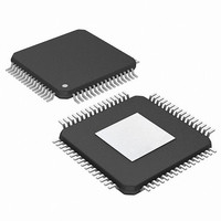
PIC24FJ256DA210T-I/BG Microchip Technology, PIC24FJ256DA210T-I/BG Datasheet - Page 31

PIC24FJ256DA210T-I/BG
Manufacturer Part Number
PIC24FJ256DA210T-I/BG
Description
16-bit, 256KB Flash, 96K RAM, USB, Graphics 121 XBGA 10x10x1.20mm T/R
Manufacturer
Microchip Technology
Series
PIC® 24Fr
Specifications of PIC24FJ256DA210T-I/BG
Core Processor
PIC
Core Size
16-Bit
Speed
32MHz
Connectivity
I²C, IrDA, SPI, UART/USART, USB OTG
Peripherals
Brown-out Detect/Reset, GFX, LVD, POR, PWM, WDT
Number Of I /o
84
Program Memory Size
256KB (85.5K x 24)
Program Memory Type
FLASH
Ram Size
96K x 8
Voltage - Supply (vcc/vdd)
2.2 V ~ 3.6 V
Data Converters
A/D 24x10b
Oscillator Type
Internal
Operating Temperature
-40°C ~ 85°C
Package / Case
121-TFBGA
Lead Free Status / RoHS Status
Lead free / RoHS Compliant
Eeprom Size
-
Lead Free Status / RoHS Status
Lead free / RoHS Compliant
Available stocks
Company
Part Number
Manufacturer
Quantity
Price
Company:
Part Number:
PIC24FJ256DA210T-I/BG
Manufacturer:
Microchip Technology
Quantity:
10 000
- Current page: 31 of 408
- Download datasheet (4Mb)
TABLE 1-3:
2010 Microchip Technology Inc.
TCK
TDI
TDO
TMS
USBID
USBOEN
V
V
V
V
V
V
V
V
V
V
VMIO
VPIO
V
V
V
V
V
Legend:
Note 1:
Function
BUS
BUSCHG
BUSON
BUSST
BUSVLD
CAP
CMPST
CMPST
CPCON
DD
REF
REF
SS
SYNC
USB
-
+
2:
3:
4:
1
2
TTL = TTL input buffer
ANA = Analog level input/output
The alternate EPMP pins are selected when the ALTPMP (CW3<12>) bit is programmed to ‘0’.
The PMSC2 signal will replace the PMA15 signal on the 15-pin PMA when CSF<1:0> = 01 or 10.
The PMCS1 signal will replace the PMA14 signal on the 14-pin PMA when CSF<1:0> = 10.
The alternate V
TQFP/QFN
10, 26, 38
9, 25, 41
64-Pin
27
28
24
23
33
12
34
49
58
58
56
58
59
49
14
13
15
16
35
11
1
PIC24FJ256DA210 FAMILY PINOUT DESCRIPTIONS (CONTINUED)
Pin Number
REF
15, 36, 45,
2, 16, 37,
28, 24
29, 25
100-Pin
46, 62
65, 75
TQFP
pins selected when the ALTVREF (CW1<5>) bit is programmed to ‘0’.
38
60
61
17
51
21
54
76
20
87
87
85
87
88
76
23
22
96
55
(4)
(4)
G7, H3, D4,
G5, H6, K8,
C2, C9, F8,
K3, K2
L2, K1
B10, F5,
F10, G6,
121-Pin
H4, E5
BGA
G11
K10
A11
A11
G9
G3
H2
H8
H1
B6
B6
B7
B6
A6
D5
C3
H9
J6
J2
J1
(4)
(4)
PIC24FJ256DA210 FAMILY
I/O
O
O
O
O
P
O
P
P
O
P
I
I
I
I
I
I
I
I
I
I
I
I
I
Buffer
Input
ANA
ANA
ANA
ANA
ST
ST
ST
ST
—
—
ST
ST
ST
ST
ST
—
ST = Schmitt Trigger input buffer
I
—
—
—
—
—
—
—
2
C™ = I
JTAG Test Clock Input.
JTAG Test Data Input.
JTAG Test Data Output.
JTAG Test Mode Select Input.
USB OTG ID (OTG mode only).
USB Output Enable Control (for external transceiver).
USB Voltage, Host mode (5V).
External USB V
USB OTG External Charge Pump Control.
USB OTG Internal Charge Pump Feedback Control.
USB V
External Filter Capacitor Connection (regulator enabled).
USB V
USB V
USB OTG V
Positive Supply for Peripheral Digital Logic and I/O Pins.
USB Differential Minus Input/Output (external transceiver).
USB Differential Plus Input/Output (external transceiver).
A/D and Comparator Reference Voltage (low) Input.
A/D and Comparator Reference Voltage (high) Input.
Ground Reference for Logic and I/O Pins.
Graphics Display Vertical Sync Pulse.
USB Voltage (3.3V).
2
C/SMBus input buffer
BUS
BUS
BUS
Boost Generator, Comparator Input 1.
Boost Generator, Comparator Input 1.
Boost Generator, Comparator Input 2.
BUS
BUS
PWM/Charge Output.
Charge Output.
Description
DS39969B-page 31
Related parts for PIC24FJ256DA210T-I/BG
Image
Part Number
Description
Manufacturer
Datasheet
Request
R

Part Number:
Description:
Manufacturer:
Microchip Technology Inc.
Datasheet:

Part Number:
Description:
Manufacturer:
Microchip Technology Inc.
Datasheet:

Part Number:
Description:
Manufacturer:
Microchip Technology Inc.
Datasheet:

Part Number:
Description:
Manufacturer:
Microchip Technology Inc.
Datasheet:

Part Number:
Description:
Manufacturer:
Microchip Technology Inc.
Datasheet:

Part Number:
Description:
Manufacturer:
Microchip Technology Inc.
Datasheet:

Part Number:
Description:
Manufacturer:
Microchip Technology Inc.
Datasheet:

Part Number:
Description:
Manufacturer:
Microchip Technology Inc.
Datasheet:


