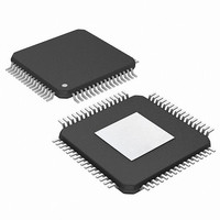
PIC24FJ256DA210T-I/BG Microchip Technology, PIC24FJ256DA210T-I/BG Datasheet - Page 324

PIC24FJ256DA210T-I/BG
Manufacturer Part Number
PIC24FJ256DA210T-I/BG
Description
16-bit, 256KB Flash, 96K RAM, USB, Graphics 121 XBGA 10x10x1.20mm T/R
Manufacturer
Microchip Technology
Series
PIC® 24Fr
Specifications of PIC24FJ256DA210T-I/BG
Core Processor
PIC
Core Size
16-Bit
Speed
32MHz
Connectivity
I²C, IrDA, SPI, UART/USART, USB OTG
Peripherals
Brown-out Detect/Reset, GFX, LVD, POR, PWM, WDT
Number Of I /o
84
Program Memory Size
256KB (85.5K x 24)
Program Memory Type
FLASH
Ram Size
96K x 8
Voltage - Supply (vcc/vdd)
2.2 V ~ 3.6 V
Data Converters
A/D 24x10b
Oscillator Type
Internal
Operating Temperature
-40°C ~ 85°C
Package / Case
121-TFBGA
Lead Free Status / RoHS Status
Lead free / RoHS Compliant
Eeprom Size
-
Lead Free Status / RoHS Status
Lead free / RoHS Compliant
Available stocks
Company
Part Number
Manufacturer
Quantity
Price
Company:
Part Number:
PIC24FJ256DA210T-I/BG
Manufacturer:
Microchip Technology
Quantity:
10 000
- Current page: 324 of 408
- Download datasheet (4Mb)
PIC24FJ256DA210 FAMILY
22.2
The PIC24FJ256DA210 family of devices has two vari-
ants in terms of on-board RAM (24-Kbyte and 96-Kbyte
variants). The 24-Kbyte variant supports monochrome
displays while the 96-Kbyte variant supports Quarter
VGA (QVGA) color displays, up to 256 colors. Support of
higher resolution displays with higher color depth
requirements are available by extending the data space
through external memory. Table 22-1 provides the sum-
mary of image buffer memory requirements of different
display resolutions and color depth requirements.
22.3
Frequency of the Graphics Controller Display Clock
(GCLK) signal is determined by programming the
GCLKDIV bits (CLKDIV2<15:9>). For more informa-
tion, refer to the “PIC24F Family Reference Manual”,
Section 6. “Oscillator” (DS39700).
TABLE 22-1:
DS39969B-page 324
480x272 (WQVGA)
320x240 (QVGA)
240x160 (HQVGA)
160x160
160x120 (QQVGA)
128x64
Legend:
Display Resolution
Display Resolution and Memory
Requirements
Display Clock (GCLK) Source
BUFFER MEMORY REQUIREMENTS vs. DISPLAY CONFIGURATION
Less than 24-Kbyte RAM variants (PIC24FJXXXDA106)
Less than 96-Kbyte RAM variants (PIC24FJXXXDA2XX)
External Memory with 96 Kbytes/24 Kbytes of RAM variants (PIC24FJXXXDAX10)
1 Bpp
16320
9600
4800
3200
2400
1024
Display Buffer Memory Requirements (Bytes)
2 Bpp
32640
19200
9600
6400
4800
2048
22.4
The PIC24FJ256DA210 family of devices has variants
with two on-board RAM sizes. These are the 24-Kbyte
and 96-Kbyte variants. These two RAM variants are
further divided in terms of pin counts. The 100-pin
count device will have the EPMP module available for
extending RAM for applications. The 64-pin count
device will not have the EPMP modules. Extending the
RAM size is necessary for applications that require
larger display buffers and work areas. It is recom-
mended that the display buffers and work areas are not
mapped into an area that overlaps the internal RAM
and the external RAM. The external RAM can be
interfaced using the EPMP module. For details, refer to
the “PIC24F Family Reference Manual”, Section 42.
“Enhanced
(DS39730).
Display Buffer and Work Areas
Memory Locations
4 Bpp
65280
38400
19200
12800
9600
4096
Parallel
2010 Microchip Technology Inc.
130560
8 Bpp
76800
38400
25600
19200
Master
8192
Port
16 Bpp
153600
261120
76800
51200
38400
16384
(EPMP)”
Related parts for PIC24FJ256DA210T-I/BG
Image
Part Number
Description
Manufacturer
Datasheet
Request
R

Part Number:
Description:
Manufacturer:
Microchip Technology Inc.
Datasheet:

Part Number:
Description:
Manufacturer:
Microchip Technology Inc.
Datasheet:

Part Number:
Description:
Manufacturer:
Microchip Technology Inc.
Datasheet:

Part Number:
Description:
Manufacturer:
Microchip Technology Inc.
Datasheet:

Part Number:
Description:
Manufacturer:
Microchip Technology Inc.
Datasheet:

Part Number:
Description:
Manufacturer:
Microchip Technology Inc.
Datasheet:

Part Number:
Description:
Manufacturer:
Microchip Technology Inc.
Datasheet:

Part Number:
Description:
Manufacturer:
Microchip Technology Inc.
Datasheet:


