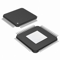
PIC24FJ256DA210T-I/BG Microchip Technology, PIC24FJ256DA210T-I/BG Datasheet - Page 342

PIC24FJ256DA210T-I/BG
Manufacturer Part Number
PIC24FJ256DA210T-I/BG
Description
16-bit, 256KB Flash, 96K RAM, USB, Graphics 121 XBGA 10x10x1.20mm T/R
Manufacturer
Microchip Technology
Series
PIC® 24Fr
Specifications of PIC24FJ256DA210T-I/BG
Core Processor
PIC
Core Size
16-Bit
Speed
32MHz
Connectivity
I²C, IrDA, SPI, UART/USART, USB OTG
Peripherals
Brown-out Detect/Reset, GFX, LVD, POR, PWM, WDT
Number Of I /o
84
Program Memory Size
256KB (85.5K x 24)
Program Memory Type
FLASH
Ram Size
96K x 8
Voltage - Supply (vcc/vdd)
2.2 V ~ 3.6 V
Data Converters
A/D 24x10b
Oscillator Type
Internal
Operating Temperature
-40°C ~ 85°C
Package / Case
121-TFBGA
Lead Free Status / RoHS Status
Lead free / RoHS Compliant
Eeprom Size
-
Lead Free Status / RoHS Status
Lead free / RoHS Compliant
Available stocks
Company
Part Number
Manufacturer
Quantity
Price
Company:
Part Number:
PIC24FJ256DA210T-I/BG
Manufacturer:
Microchip Technology
Quantity:
10 000
- Current page: 342 of 408
- Download datasheet (4Mb)
PIC24FJ256DA210 FAMILY
REGISTER 25-1:
DS39969B-page 342
bit 15
bit 7
Legend:
R = Readable bit
-n = Value at POR
bit 15-11
bit 10
bit 9-8
bit 7
bit 6
bit 5
bit 4
bit 3-0
CVREN
R/W-0
U-0
—
Unimplemented: Read as ‘0’
CVREFP: Voltage Reference Select bit (valid only when CREF is ‘1’)
1 = V
0 = The CVR (4-bit DAC) within this module provides the the reference voltage to the comparators
CVREFM<1:0>: Band Gap Reference Source Select bits (valid only when CCH<1:0> = 11)
00 = Band gap voltage is provided as an input to the comparators
01 = Band gap voltage divided-by-two is provided as an input to the comparators
10 = Band gap voltage divided-by-six is provided as an input to the comparators
11 = V
CVREN: Comparator Voltage Reference Enable bit
1 = CV
0 = CV
CVROE: Comparator V
1 = CVREF voltage level is output on the CV
0 = CVREF voltage level is disconnected from the CV
CVRR: Comparator V
1 = CV
0 = CV
CVRSS: Comparator V
1 = Comparator reference source CV
0 = Comparator reference source CV
CVR<3:0>: Comparator V
When CVRR = 1:
CV
When CVRR = 0:
CV
CVROE
REF
REF
R/W-0
U-0
—
REF
CVRCON: COMPARATOR VOLTAGE REFERENCE CONTROL REGISTER
= (CVR<3:0>/ 24) (CV
= 1/4 (CV
REF
REF
REF
RSRC
RSRC
+ is used as a reference voltage to the comparators
+ pin is provided as an input the comparators
circuit is powered on
circuit is powered down
range should be 0 to 0.625 CV
range should be 0.25 to 0.719 CV
W = Writable bit
‘1’ = Bit is set
R/W-0
CVRR
RSRC
U-0
—
REF
REF
REF
) + (CVR<3:0>/32) (CV
Range Selection bit
REF
Source Selection bit
Output Enable bit
Value Selection 0 CVR<3:0> 15 bits
RSRC
CVRSS
R/W-0
U-0
—
)
RSRC
RSRC
= V
= AV
RSRC
U = Unimplemented bit, read as ‘0’
‘0’ = Bit is cleared
REF
REF
RSRC
R/W-0
CVR3
DD
RSRC
U-0
pin
—
with CV
+ – V
– AV
with CV
)
REF
REF
SS
RSRC
pin
-
RSRC
CVREFP
R/W-0
R/W-0
CVR2
/24 step size
/32 step size
2010 Microchip Technology Inc.
x = Bit is unknown
CVREFM1
R/W-0
R/W-0
CVR1
CVREFM0
R/W-0
R/W-0
CVR0
bit 8
bit 0
Related parts for PIC24FJ256DA210T-I/BG
Image
Part Number
Description
Manufacturer
Datasheet
Request
R

Part Number:
Description:
Manufacturer:
Microchip Technology Inc.
Datasheet:

Part Number:
Description:
Manufacturer:
Microchip Technology Inc.
Datasheet:

Part Number:
Description:
Manufacturer:
Microchip Technology Inc.
Datasheet:

Part Number:
Description:
Manufacturer:
Microchip Technology Inc.
Datasheet:

Part Number:
Description:
Manufacturer:
Microchip Technology Inc.
Datasheet:

Part Number:
Description:
Manufacturer:
Microchip Technology Inc.
Datasheet:

Part Number:
Description:
Manufacturer:
Microchip Technology Inc.
Datasheet:

Part Number:
Description:
Manufacturer:
Microchip Technology Inc.
Datasheet:


