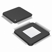
PIC24FJ256DA210T-I/BG Microchip Technology, PIC24FJ256DA210T-I/BG Datasheet - Page 78

PIC24FJ256DA210T-I/BG
Manufacturer Part Number
PIC24FJ256DA210T-I/BG
Description
16-bit, 256KB Flash, 96K RAM, USB, Graphics 121 XBGA 10x10x1.20mm T/R
Manufacturer
Microchip Technology
Series
PIC® 24Fr
Specifications of PIC24FJ256DA210T-I/BG
Core Processor
PIC
Core Size
16-Bit
Speed
32MHz
Connectivity
I²C, IrDA, SPI, UART/USART, USB OTG
Peripherals
Brown-out Detect/Reset, GFX, LVD, POR, PWM, WDT
Number Of I /o
84
Program Memory Size
256KB (85.5K x 24)
Program Memory Type
FLASH
Ram Size
96K x 8
Voltage - Supply (vcc/vdd)
2.2 V ~ 3.6 V
Data Converters
A/D 24x10b
Oscillator Type
Internal
Operating Temperature
-40°C ~ 85°C
Package / Case
121-TFBGA
Lead Free Status / RoHS Status
Lead free / RoHS Compliant
Eeprom Size
-
Lead Free Status / RoHS Status
Lead free / RoHS Compliant
Available stocks
Company
Part Number
Manufacturer
Quantity
Price
Company:
Part Number:
PIC24FJ256DA210T-I/BG
Manufacturer:
Microchip Technology
Quantity:
10 000
- Current page: 78 of 408
- Download datasheet (4Mb)
PIC24FJ256DA210 FAMILY
4.3.3
The upper 32 Kbytes of data space may optionally be
mapped into any 16K word page of the program space.
This provides transparent access of stored constant
data from the data space without the need to use
special instructions (i.e., TBLRDL/H).
Program space access through the data space occurs
when the MSb of EA is ‘1’ and the DSRPAG<9> is also
‘1’. The lower 8 bits of DSRPAG are concatenated to the
Wn<14:0> bits to form a 23-bit EA to access program
memory. The DSRPAG<8> decides which word should
be addressed; when the bit is ‘0’, the lower word and
when ‘1’, the upper word of the program memory is
accessed.
The entire program memory is divided into 512 EDS
pages, from 0x200 to 0x3FF, each consisting of 16K
words of data. Pages, 0x200 to 0x2FF, correspond to
the lower words of the program memory, while 0x300 to
0x3FF correspond to the upper words of the program
memory.
Using this EDS technique, the entire program memory
can be accessed. Previously, the access to the upper
word of the program memory was not supported.
TABLE 4-37:
DS39969B-page 78
Note 1:
(Data Space Read Register)
DSRPAG
When the source/destination address is above 0x8000 and DSRPAG/DSWPAG is ‘0’, an address error
trap will occur.
READING DATA FROM PROGRAM
MEMORY USING EDS
0x2FF
0x3FF
0x200
0x300
0x000
•
•
•
•
•
•
EDS PROGRAM ADDRESS WITH DIFFERENT PAGES AND ADDRESSES
0x8000 to 0xFFFF
Source Address
while Indirect
Addressing
23-Bit EA Pointing to EDS
0x7F8000 to 0x7FFFFE
0x7F8001 to 0x7FFFFF
0x000000 to 0x007FFE
0x000001 to 0x007FFF
Table 4-37 provides the corresponding 23-bit EDS
address for program memory with EDS page and
source addresses.
For operations that use PSV and are executed outside
a REPEAT loop, the MOV and MOV.D instructions will
require one instruction cycle in addition to the specified
execution time. All other instructions will require two
instruction cycles in addition to the specified execution
time.
For operations that use PSV, which are executed inside
a REPEAT loop, there will be some instances that
require two instruction cycles in addition to the
specified execution time of the instruction:
• Execution in the first iteration
• Execution in the last iteration
• Execution prior to exiting the loop due to an
• Execution upon re-entering the loop after an
Any other iteration of the REPEAT loop will allow the
instruction accessing data, using PSV, to execute in a
single cycle.
Invalid Address
interrupt
interrupt is serviced
•
•
•
•
•
•
2010 Microchip Technology Inc.
Lower words of 4M
program instructions;
(8 Mbytes) for read
operations only.
Upper words of 4M
program instructions
(4 Mbytes remaining,
4 Mbytes are phantom
bytes) for read
operations only.
Address error trap
Comment
(1)
Related parts for PIC24FJ256DA210T-I/BG
Image
Part Number
Description
Manufacturer
Datasheet
Request
R

Part Number:
Description:
Manufacturer:
Microchip Technology Inc.
Datasheet:

Part Number:
Description:
Manufacturer:
Microchip Technology Inc.
Datasheet:

Part Number:
Description:
Manufacturer:
Microchip Technology Inc.
Datasheet:

Part Number:
Description:
Manufacturer:
Microchip Technology Inc.
Datasheet:

Part Number:
Description:
Manufacturer:
Microchip Technology Inc.
Datasheet:

Part Number:
Description:
Manufacturer:
Microchip Technology Inc.
Datasheet:

Part Number:
Description:
Manufacturer:
Microchip Technology Inc.
Datasheet:

Part Number:
Description:
Manufacturer:
Microchip Technology Inc.
Datasheet:


