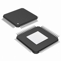
PIC24FJ256DA210T-I/BG Microchip Technology, PIC24FJ256DA210T-I/BG Datasheet - Page 86

PIC24FJ256DA210T-I/BG
Manufacturer Part Number
PIC24FJ256DA210T-I/BG
Description
16-bit, 256KB Flash, 96K RAM, USB, Graphics 121 XBGA 10x10x1.20mm T/R
Manufacturer
Microchip Technology
Series
PIC® 24Fr
Specifications of PIC24FJ256DA210T-I/BG
Core Processor
PIC
Core Size
16-Bit
Speed
32MHz
Connectivity
I²C, IrDA, SPI, UART/USART, USB OTG
Peripherals
Brown-out Detect/Reset, GFX, LVD, POR, PWM, WDT
Number Of I /o
84
Program Memory Size
256KB (85.5K x 24)
Program Memory Type
FLASH
Ram Size
96K x 8
Voltage - Supply (vcc/vdd)
2.2 V ~ 3.6 V
Data Converters
A/D 24x10b
Oscillator Type
Internal
Operating Temperature
-40°C ~ 85°C
Package / Case
121-TFBGA
Lead Free Status / RoHS Status
Lead free / RoHS Compliant
Eeprom Size
-
Lead Free Status / RoHS Status
Lead free / RoHS Compliant
Available stocks
Company
Part Number
Manufacturer
Quantity
Price
Company:
Part Number:
PIC24FJ256DA210T-I/BG
Manufacturer:
Microchip Technology
Quantity:
10 000
- Current page: 86 of 408
- Download datasheet (4Mb)
PIC24FJ256DA210 FAMILY
5.6.2
If a Flash location has been erased, it can be pro-
grammed using table write instructions to write an
instruction word (24-bit) into the write latch. The
TBLPAG register is loaded with the 8 Most Significant
Bytes (MSB) of the Flash address. The TBLWTL and
TBLWTH instructions write the desired data into the
EXAMPLE 5-5:
EXAMPLE 5-6:
DS39969B-page 86
; Setup a pointer to data Program Memory
; Setup NVMCON for programming one word to data Program Memory
// C example using MPLAB C30
unsigned int offset;
unsigned long progAddr = 0xXXXXXX;
unsigned int progDataL = 0xXXXX;
unsigned char progDataH = 0xXX;
//Set up NVMCON for word programming
NVMCON = 0x4003;
//Set up pointer to the first memory location to be written
TBLPAG = progAddr>>16;
offset = progAddr & 0xFFFF;
//Perform TBLWT instructions to write latches
__builtin_tblwtl(offset, progDataL);
__builtin_tblwth(offset, progDataH);
asm(“DISI #5”);
__builtin_write_NVM();
MOV
MOV
MOV
MOV
MOV
TBLWTL W2, [W0]
TBLWTH W3, [W0++]
MOV
MOV
DISI
MOV.B
MOV
MOV.B
MOV
BSET
NOP
NOP
PROGRAMMING A SINGLE WORD
OF FLASH PROGRAM MEMORY
#tblpage(PROG_ADDR), W0
W0, TBLPAG
#tbloffset(PROG_ADDR), W0
#LOW_WORD_N, W2
#HIGH_BYTE_N, W3
#0x4003, W0
W0, NVMCON
#5
#0x55, W0
W0, NVMKEY
#0xAA, W0
W0, NVMKEY
NVMCON, #WR
PROGRAMMING A SINGLE WORD OF FLASH PROGRAM MEMORY
PROGRAMMING A SINGLE WORD OF FLASH PROGRAM MEMORY
(‘C’ LANGUAGE CODE)
;
;Initialize PM Page Boundary SFR
;Initialize a register with program memory address
;
;
; Write PM low word into program latch
; Write PM high byte into program latch
;
; Set NVMOP bits to 0011
; Disable interrupts while the KEY sequence is written
; Write the key sequence
; Start the write cycle
; Required delays
// Address of word to program
// Data to program lower word
// Write to address low word
// Write to upper byte
// Data to program upper byte
// Initialize NVMCON
// Initialize PM Page Boundary SFR
// Initialize lower word of address
// Block interrupts with priority <7
// for next 5 instructions
// C30 function to perform unlock
// sequence and set WR
write latches and specify the lower 16 bits of the pro-
gram memory address to write to. To configure the
NVMCON register for a word write, set the NVMOP bits
(NVMCON<3:0>) to ‘0011’. The write is performed by
executing the unlock sequence and setting the WR bit
(see Example 5-5). An equivalent procedure in ‘C’
compiler, using the MPLAB C30 compiler and built-in
hardware functions is shown in Example 5-6.
2010 Microchip Technology Inc.
Related parts for PIC24FJ256DA210T-I/BG
Image
Part Number
Description
Manufacturer
Datasheet
Request
R

Part Number:
Description:
Manufacturer:
Microchip Technology Inc.
Datasheet:

Part Number:
Description:
Manufacturer:
Microchip Technology Inc.
Datasheet:

Part Number:
Description:
Manufacturer:
Microchip Technology Inc.
Datasheet:

Part Number:
Description:
Manufacturer:
Microchip Technology Inc.
Datasheet:

Part Number:
Description:
Manufacturer:
Microchip Technology Inc.
Datasheet:

Part Number:
Description:
Manufacturer:
Microchip Technology Inc.
Datasheet:

Part Number:
Description:
Manufacturer:
Microchip Technology Inc.
Datasheet:

Part Number:
Description:
Manufacturer:
Microchip Technology Inc.
Datasheet:


