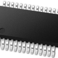
PIC24FJ64GB002-I/SS Microchip Technology, PIC24FJ64GB002-I/SS Datasheet - Page 177

PIC24FJ64GB002-I/SS
Manufacturer Part Number
PIC24FJ64GB002-I/SS
Description
16-bit, 16 MIPS, 64KB Flash, 8KB RAM, Nanowatt XLP, USB OTG 28 SSOP .209in TUBE
Manufacturer
Microchip Technology
Specifications of PIC24FJ64GB002-I/SS
Processor Series
PIC24
Core
PIC24F
Data Bus Width
16 bit
Program Memory Type
Flash
Program Memory Size
64 KB
Data Ram Size
8192 B
Interface Type
I2C, SPI, UART
Maximum Clock Frequency
32 MHz
Number Of Programmable I/os
21
Number Of Timers
5
Operating Supply Voltage
2 V to 3.6 V
Maximum Operating Temperature
+ 85 C
Mounting Style
SMD/SMT
Package / Case
SSOP-28
Development Tools By Supplier
MPLAB Integrated Development Environment
Minimum Operating Temperature
- 40 C
Operating Temperature Range
- 40 C to + 85 C
Supply Current (max)
300 mA
Lead Free Status / Rohs Status
Lead free / RoHS Compliant
Available stocks
Company
Part Number
Manufacturer
Quantity
Price
Part Number:
PIC24FJ64GB002-I/SS
Manufacturer:
MICROCHIP/微芯
Quantity:
20 000
- Current page: 177 of 352
- Download datasheet (3Mb)
REGISTER 15-2:
REGISTER 15-3:
2010 Microchip Technology Inc.
bit 4-2
bit 1-0
Note 1:
bit 15
bit 7
Legend:
R = Readable bit
-n = Value at POR
bit 15
bit 14
bit 13
bit 12-2
bit 1
bit 0
FRMEN
R/W-0
U-0
—
2:
3:
4:
If DISSCK = 0, SCKx must be configured to an available RPn pin. See Section 10.4 “Peripheral Pin
Select (PPS)” for more information.
If DISSDO = 0, SDOx must be configured to an available RPn pin. See Section 10.4 “Peripheral Pin
Select (PPS)” for more information.
The CKE bit is not used in the Framed SPI modes. The user should program this bit to ‘0’ for the Framed
SPI modes (FRMEN = 1).
If SSEN = 1, SSx must be configured to an available RPn pin. See Section 10.4 “Peripheral Pin Select
(PPS)” for more information.
SPRE<2:0>: Secondary Prescale bits (Master mode)
111 = Secondary prescale 1:1
110 = Secondary prescale 2:1
...
000 = Secondary prescale 8:1
PPRE<1:0>: Primary Prescale bits (Master mode)
11 = Primary prescale 1:1
10 = Primary prescale 4:1
01 = Primary prescale 16:1
00 = Primary prescale 64:1
FRMEN: Framed SPIx Support bit
1 = Framed SPIx support enabled
0 = Framed SPIx support disabled
SPIFSD: Frame Sync Pulse Direction Control on SSx Pin bit
1 = Frame sync pulse input (slave)
0 = Frame sync pulse output (master)
SPIFPOL: Frame Sync Pulse Polarity bit (Frame mode only)
1 = Frame sync pulse is active-high
0 = Frame sync pulse is active-low
Unimplemented: Read as ‘0’
SPIFE: Frame Sync Pulse Edge Select bit
1 = Frame sync pulse coincides with first bit clock
0 = Frame sync pulse precedes first bit clock
SPIBEN: Enhanced Buffer Enable bit
1 = Enhanced buffer enabled
0 = Enhanced buffer disabled (Legacy mode)
SPIFSD
R/W-0
U-0
—
SPI
SPIxCON2: SPIx CONTROL REGISTER 2
X
CON1: SPIx CONTROL REGISTER 1 (CONTINUED)
W = Writable bit
‘1’ = Bit is set
SPIFPOL
R/W-0
U-0
—
U-0
U-0
PIC24FJ64GB004 FAMILY
—
—
U = Unimplemented bit, read as ‘0’
‘0’ = Bit is cleared
U-0
U-0
—
—
U-0
U-0
—
—
x = Bit is unknown
SPIFE
R/W-0
U-0
—
DS39940D-page 177
SPIBEN
R/W-0
U-0
—
bit 8
bit 0
Related parts for PIC24FJ64GB002-I/SS
Image
Part Number
Description
Manufacturer
Datasheet
Request
R

Part Number:
Description:
Manufacturer:
Microchip Technology Inc.
Datasheet:

Part Number:
Description:
Manufacturer:
Microchip Technology Inc.
Datasheet:

Part Number:
Description:
Manufacturer:
Microchip Technology Inc.
Datasheet:

Part Number:
Description:
Manufacturer:
Microchip Technology Inc.
Datasheet:

Part Number:
Description:
Manufacturer:
Microchip Technology Inc.
Datasheet:

Part Number:
Description:
Manufacturer:
Microchip Technology Inc.
Datasheet:

Part Number:
Description:
Manufacturer:
Microchip Technology Inc.
Datasheet:

Part Number:
Description:
Manufacturer:
Microchip Technology Inc.
Datasheet:


