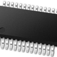
PIC24FJ64GB002-I/SS Microchip Technology, PIC24FJ64GB002-I/SS Datasheet - Page 192

PIC24FJ64GB002-I/SS
Manufacturer Part Number
PIC24FJ64GB002-I/SS
Description
16-bit, 16 MIPS, 64KB Flash, 8KB RAM, Nanowatt XLP, USB OTG 28 SSOP .209in TUBE
Manufacturer
Microchip Technology
Specifications of PIC24FJ64GB002-I/SS
Processor Series
PIC24
Core
PIC24F
Data Bus Width
16 bit
Program Memory Type
Flash
Program Memory Size
64 KB
Data Ram Size
8192 B
Interface Type
I2C, SPI, UART
Maximum Clock Frequency
32 MHz
Number Of Programmable I/os
21
Number Of Timers
5
Operating Supply Voltage
2 V to 3.6 V
Maximum Operating Temperature
+ 85 C
Mounting Style
SMD/SMT
Package / Case
SSOP-28
Development Tools By Supplier
MPLAB Integrated Development Environment
Minimum Operating Temperature
- 40 C
Operating Temperature Range
- 40 C to + 85 C
Supply Current (max)
300 mA
Lead Free Status / Rohs Status
Lead free / RoHS Compliant
Available stocks
Company
Part Number
Manufacturer
Quantity
Price
Part Number:
PIC24FJ64GB002-I/SS
Manufacturer:
MICROCHIP/微芯
Quantity:
20 000
- Current page: 192 of 352
- Download datasheet (3Mb)
PIC24FJ64GB004 FAMILY
REGISTER 17-1:
DS39940D-page 192
bit 15
bit 7
Legend:
R = Readable bit
-n = Value at POR
bit 15
bit 14
bit 13
bit 12
bit 11
bit 10
bit 9-8
bit 7
bit 6
bit 5
bit 4
Note 1:
UARTEN
R/W-0, HC
R/W-0
WAKE
2:
(1)
If UARTEN = 1, the peripheral inputs and outputs must be configured to an available RPn pin. See
Section 10.4 “Peripheral Pin Select (PPS)” for more information.
This feature is only available for the 16x BRG mode (BRGH = 0).
UARTEN: UARTx Enable bit
1 = UARTx is enabled; all UARTx pins are controlled by UARTx as defined by UEN<1:0>
0 = UARTx is disabled; all UARTx pins are controlled by port latches; UARTx power consumption is minimal
Unimplemented: Read as ‘0’
USIDL: Stop in Idle Mode bit
1 = Discontinue module operation when the device enters Idle mode
0 = Continue module operation in Idle mode
IREN: IrDA
1 = IrDA encoder and decoder enabled
0 = IrDA encoder and decoder disabled
RTSMD: Mode Selection for UxRTS Pin bit
1 = UxRTS pin in Simplex mode
0 = UxRTS pin in Flow Control mode
Unimplemented: Read as ‘0’
UEN<1:0>: UARTx Enable bits
11 = UxTX, UxRX and BCLKx pins are enabled and used; UxCTS pin controlled by port latches
10 = UxTX, UxRX, UxCTS and UxRTS pins are enabled and used
01 = UxTX, UxRX and UxRTS pins are enabled and used; UxCTS pin controlled by port latches
00 = UxTX and UxRX pins are enabled and used; UxCTS and UxRTS/BCLKx pins controlled by port
WAKE: Wake-up on Start Bit Detect During Sleep Mode Enable bit
1 = UARTx will continue to sample the UxRX pin; interrupt generated on falling edge; bit cleared in
0 = No wake-up enabled
LPBACK: UARTx Loopback Mode Select bit
1 = Enable Loopback mode
0 = Loopback mode is disabled
ABAUD: Auto-Baud Enable bit
1 = Enable baud rate measurement on the next character – requires reception of a Sync field (55h);
0 = Baud rate measurement disabled or completed
RXINV: Receive Polarity Inversion bit
1 = UxRX Idle state is ‘0’
0 = UxRX Idle state is ‘1’
LPBACK
R/W-0
U-0
hardware on following rising edge
cleared in hardware upon completion
—
latches
UxMODE: UARTx MODE REGISTER
®
Encoder and Decoder Enable bit
HC = Hardware Clearable bit
W = Writable bit
‘1’ = Bit is set
R/W-0, HC
ABAUD
USIDL
R/W-0
(1)
IREN
RXINV
R/W-0
R/W-0
(2)
U = Unimplemented bit, read as ‘0’
‘0’ = Bit is cleared
(2)
RTSMD
R/W-0
R/W-0
BRGH
PDSEL1
R/W-0
U-0
—
2010 Microchip Technology Inc.
x = Bit is unknown
PDSEL0
R/W-0
R/W-0
UEN1
STSEL
R/W-0
R/W-0
UEN0
bit 8
bit 0
Related parts for PIC24FJ64GB002-I/SS
Image
Part Number
Description
Manufacturer
Datasheet
Request
R

Part Number:
Description:
Manufacturer:
Microchip Technology Inc.
Datasheet:

Part Number:
Description:
Manufacturer:
Microchip Technology Inc.
Datasheet:

Part Number:
Description:
Manufacturer:
Microchip Technology Inc.
Datasheet:

Part Number:
Description:
Manufacturer:
Microchip Technology Inc.
Datasheet:

Part Number:
Description:
Manufacturer:
Microchip Technology Inc.
Datasheet:

Part Number:
Description:
Manufacturer:
Microchip Technology Inc.
Datasheet:

Part Number:
Description:
Manufacturer:
Microchip Technology Inc.
Datasheet:

Part Number:
Description:
Manufacturer:
Microchip Technology Inc.
Datasheet:


