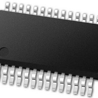
PIC24FJ64GB002-I/SS Microchip Technology, PIC24FJ64GB002-I/SS Datasheet - Page 30

PIC24FJ64GB002-I/SS
Manufacturer Part Number
PIC24FJ64GB002-I/SS
Description
16-bit, 16 MIPS, 64KB Flash, 8KB RAM, Nanowatt XLP, USB OTG 28 SSOP .209in TUBE
Manufacturer
Microchip Technology
Specifications of PIC24FJ64GB002-I/SS
Processor Series
PIC24
Core
PIC24F
Data Bus Width
16 bit
Program Memory Type
Flash
Program Memory Size
64 KB
Data Ram Size
8192 B
Interface Type
I2C, SPI, UART
Maximum Clock Frequency
32 MHz
Number Of Programmable I/os
21
Number Of Timers
5
Operating Supply Voltage
2 V to 3.6 V
Maximum Operating Temperature
+ 85 C
Mounting Style
SMD/SMT
Package / Case
SSOP-28
Development Tools By Supplier
MPLAB Integrated Development Environment
Minimum Operating Temperature
- 40 C
Operating Temperature Range
- 40 C to + 85 C
Supply Current (max)
300 mA
Lead Free Status / Rohs Status
Lead free / RoHS Compliant
Available stocks
Company
Part Number
Manufacturer
Quantity
Price
Part Number:
PIC24FJ64GB002-I/SS
Manufacturer:
MICROCHIP/微芯
Quantity:
20 000
- Current page: 30 of 352
- Download datasheet (3Mb)
PIC24FJ64GB004 FAMILY
3.3.2
The divide block supports signed and unsigned integer
divide operations with the following data sizes:
1.
2.
3.
4.
The quotient for all divide instructions ends up in W0
and the remainder in W1. Sixteen-bit signed and
unsigned DIV instructions can specify any W register
for both the 16-bit divisor (Wn), and any W register
(aligned) pair (W(m + 1):Wm) for the 32-bit dividend.
The divide algorithm takes one cycle per bit of divisor,
so both 32-bit/16-bit and 16-bit/16-bit instructions take
the same number of cycles to execute.
TABLE 3-2:
DS39940D-page 30
32-bit signed/16-bit signed divide
32-bit unsigned/16-bit unsigned divide
16-bit signed/16-bit signed divide
16-bit unsigned/16-bit unsigned divide
Instruction
ASR
LSR
SL
DIVIDER
INSTRUCTIONS THAT USE THE SINGLE AND MULTI-BIT SHIFT OPERATION
Arithmetic Shift Right Source Register by One or More Bits.
Shift Left Source Register by One or More Bits.
Logical Shift Right Source Register by One or More Bits.
3.3.3
The PIC24F ALU supports both single bit and
single-cycle, multi-bit arithmetic and logic shifts.
Multi-bit shifts are implemented using a shifter block,
capable of performing up to a 15-bit arithmetic right
shift, or up to a 15-bit left shift, in a single cycle. All
multi-bit shift instructions only support Register Direct
Addressing for both the operand source and result
destination.
A full summary of instructions that use the shift
operation is provided below in Table 3-2.
Description
MULTI-BIT SHIFT SUPPORT
2010 Microchip Technology Inc.
Related parts for PIC24FJ64GB002-I/SS
Image
Part Number
Description
Manufacturer
Datasheet
Request
R

Part Number:
Description:
Manufacturer:
Microchip Technology Inc.
Datasheet:

Part Number:
Description:
Manufacturer:
Microchip Technology Inc.
Datasheet:

Part Number:
Description:
Manufacturer:
Microchip Technology Inc.
Datasheet:

Part Number:
Description:
Manufacturer:
Microchip Technology Inc.
Datasheet:

Part Number:
Description:
Manufacturer:
Microchip Technology Inc.
Datasheet:

Part Number:
Description:
Manufacturer:
Microchip Technology Inc.
Datasheet:

Part Number:
Description:
Manufacturer:
Microchip Technology Inc.
Datasheet:

Part Number:
Description:
Manufacturer:
Microchip Technology Inc.
Datasheet:


