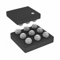
SSM2317CBZ-REEL7 Analog Devices Inc, SSM2317CBZ-REEL7 Datasheet

SSM2317CBZ-REEL7
Specifications of SSM2317CBZ-REEL7
Related parts for SSM2317CBZ-REEL7
SSM2317CBZ-REEL7 Summary of contents
Page 1
FEATURES Filterless Class-D amplifier with Σ-Δ modulation Automatic level control (ALC) improves dynamic range and prevents clipping 3 W into 3 Ω load and 1.4 W into 8 Ω load at 5.0 V supply with <10% total harmonic distortion (ALC ...
Page 2
SSM2317 TABLE OF CONTENTS Features .............................................................................................. 1 Applications ....................................................................................... 1 General Description ......................................................................... 1 Functional Block Diagram .............................................................. 1 Revision History ............................................................................... 2 Specifications ..................................................................................... 3 Absolute Maximum Ratings ............................................................ 5 Thermal Resistance ...................................................................... 5 ESD Caution .................................................................................. 5 Pin ...
Page 3
SPECIFICATIONS 25° Ω μH, ALC = off, unless otherwise noted Table 1. Parameter DEVICE CHARACTERISTICS Output Power Efficiency Total Harmonic Distortion + Noise Input Common-Mode Voltage ...
Page 4
SSM2317 Parameter NOISE PERFORMANCE Output Voltage Noise Signal-to-Noise Ratio 1 Although the SSM2317 has good audio quality above 3 W, continuous output power beyond 3 W must be avoided due to device packaging limitations. Symbol Conditions 3.6 ...
Page 5
ABSOLUTE MAXIMUM RATINGS Absolute maximum ratings apply wise noted. Table 2. Parameter Supply Voltage Input Voltage Common-Mode Input Voltage Continuous Output Power Storage Temperature Range Operating Temperature Range Junction Temperature Range Lead Temperature (Soldering, 60 sec) ESD ...
Page 6
SSM2317 PIN CONFIGURATION AND FUNCTION DESCRIPTIONS Table 4. Pin Function Descriptions Pin No. Mnemonic 1A IN− 1B IN+ 1C GND ALC_EN 2C VDD 3A VTH 3B OUT− 3C OUT+ BALL A1 CORNER ...
Page 7
TYPICAL PERFORMANCE CHARACTERISTICS 100 R = 8Ω + 33µH L GAIN = 18dB 2. 0.1 0.01 0.001 0.0001 0.001 0.01 0.1 OUTPUT POWER (W) Figure 3. THD + N vs. Output Power into ...
Page 8
SSM2317 100 V = 3.6V DD GAIN = 18dB R = 8Ω + 33µ 0.1 0.5W 0.125W 0.01 0.25W 0.001 10 100 1k FREQUENCY (Hz) Figure 9. THD + N vs. Frequency 3 ...
Page 9
R = 8Ω + 33µ 4Ω + 33µH L 3.6 3.4 NO LOAD 3.2 3.0 2.8 2.6 2.5 3.0 3.5 4.0 4.5 5.0 SUPPLY VOLTAGE (V) Figure 15. Supply Current vs. Supply Voltage ...
Page 10
SSM2317 100 3. 2. 0.2 0.4 0.6 0.8 1.0 1.2 1.4 1.6 1.8 2.0 2.2 2.4 2.6 2.8 3.0 3.2 OUTPUT POWER (W) ...
Page 11
R = 3Ω + 33µH L 900 800 700 V = 3.6V DD 600 500 V = 2.5V DD 400 300 200 100 0 0 0.2 0.4 0.6 0.8 1.0 1.2 1.4 1.6 1.8 2.0 2.2 2.4 2.6 2.8 ...
Page 12
SSM2317 3. 8Ω + 33µH L ALC = ON 1 0.1 0.01 0.001 0.01 0.1 INPUT (V rms) Figure 33. Input/Output Characteristic, V 1V/DIV INPUT OUTPUT ALC = ON V ...
Page 13
TYPICAL APPLICATION CIRCUITS EXTERNAL GAIN SETTINGS = 80kΩ/(10kΩ 0.1µF R EXT AUDIO IN+ 1 0.1µF R EXT AUDIO IN– SHUTDOWN EXTERNAL GAIN SETTINGS = 80kΩ/(10kΩ 0.1µF R EXT AUDIO IN+ 0.1µF R EXT SHUTDOWN ) ...
Page 14
SSM2317 THEORY OF OPERATION OVERVIEW The SSM2317 mono Class-D audio amplifier features a filterless modulation scheme that greatly reduces the external components count, conserving board space and, thus, reducing systems cost. The SSM2317 does not require an output filter but ...
Page 15
A multilayer board allows a complete layer to be used for the ground plane, whereas the ground plane side of a double-sided board is often disrupted with signal crossover. If the system has separate analog and ...
Page 16
SSM2317 OUTPUT THRESHOLD The maximum output amplitude threshold (V limiting mode can be changed from 90 having an external resistor between the VTH pin and GND. TH Shorting the VTH pin to GND sets ...
Page 17
... OUTLINE DIMENSIONS 1.490 1.460 SQ A1 BALL 1.430 CORNER TOP VIEW (BALL SIDE DOWN) ORDERING GUIDE Model Temperature Range 1 SSM2317CBZ-REEL −40°C to +85°C SSM2317CBZ-REEL7 1 −40°C to +85°C 1 SSM2317-EVALZ SSM2317-MINI-EVALZ RoHS Compliant Part. 0.655 0.600 0.545 SEATING PLANE 0.350 0.320 0.290 ...
Page 18
SSM2317 NOTES Rev Page ...
Page 19
NOTES Rev Page SSM2317 ...
Page 20
SSM2317 NOTES ©2008 Analog Devices, Inc. All rights reserved. Trademarks and registered trademarks are the property of their respective owners. D07242-0-6/08(A) Rev Page ...


