STB16N65M5 STMicroelectronics, STB16N65M5 Datasheet
STB16N65M5
Specifications of STB16N65M5
Available stocks


Related parts for STB16N65M5


STB16N65M5 Summary of contents
Page 1
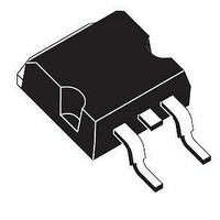
... Table 1. Device summary Order codes STB16N65M5 STD16N65M5 November 2010 R DS(on max Figure 1. Marking 16N65M5 Doc ID 18146 Rev 1 STB16N65M5 STD16N65M5 in D²PAK, DPAK DPAK D²PAK Internal schematic diagram Package Packaging D²PAK Tape and reel DPAK 3 1/16 www.st.com 16 ...
Page 2
... Contents Contents 1 Electrical ratings . . . . . . . . . . . . . . . . . . . . . . . . . . . . . . . . . . . . . . . . . . . . 3 2 Electrical characteristics . . . . . . . . . . . . . . . . . . . . . . . . . . . . . . . . . . . . . 4 2.1 Electrical characteristics (curves) 3 Test circuits 4 Package mechanical data . . . . . . . . . . . . . . . . . . . . . . . . . . . . . . . . . . . . 10 5 Packaging mechanical data . . . . . . . . . . . . . . . . . . . . . . . . . . . . . . . . . . 13 6 Revision history . . . . . . . . . . . . . . . . . . . . . . . . . . . . . . . . . . . . . . . . . . . 15 2/ Doc ID 18146 Rev 1 STB16N65M5, STD16N65M5 . . . . . . . . . . . . . . . . . . . . . . . . . . . . 6 ...
Page 3
... STB16N65M5, STD16N65M5 1 Electrical ratings Table 2. Absolute maximum ratings Symbol V Drain-source voltage ( Gate-source voltage GS I Drain current (continuous Drain current (continuous (1) I Drain current (pulsed Total dissipation at T TOT Avalanche current, repetitive or not repetitive (pulse width limited by T Single pulse avalanche energy ...
Page 4
... Max rating ± Parameter Test conditions V = 100 MHz 520 MHz open drain V = 520 (see Figure 17) DSS DSS Doc ID 18146 Rev 1 STB16N65M5, STD16N65M5 Min. Typ 650 =125 ° 250 µ 0.270 Min. Typ. 1250 - 100 = Max. Unit V 1 µA 100 µA 100 Ω ...
Page 5
... STB16N65M5, STD16N65M5 Table 6. Switching times Symbol t (v) Voltage delay time d t (v) Voltage rise time r t (i) Current fall time f t (off) Crossing time c Table 7. Source drain diode Symbol I Source-drain current SD (1) I Source-drain current (pulsed) SDM (2) V Forward on voltage SD t Reverse recovery time ...
Page 6
... Figure 3. AM08610v1 10µs 100µs 1ms 10ms V (V) 100 DS Figure 5. AM08609v1 10µs 100µs 1ms 10ms 100 V (V) DS Figure 7. AM03178v1 I D ( Doc ID 18146 Rev 1 STB16N65M5, STD16N65M5 Thermal impedance for D²PAK Thermal impedance for DPAK Transfer characteristics V =10V AM03179v1 (V) ...
Page 7
... STB16N65M5, STD16N65M5 Figure 8. Normalized B VDSS BV DSS (norm) 1.08 1.06 1.04 1.02 1.00 0.98 0.96 0.94 -50 - Figure 10. Output capacitance stored energy E oss (µ 200 400 0 100 300 Figure 12. Gate charge vs gate-source voltage Figure 13. Normalized on resistance (V) V =520V =10V = temperature Figure 9. AM03187v1 R DS(on) (Ω ...
Page 8
... Figure 14. Normalized gate threshold voltage vs temperature V GS(th) (norm) 1.10 1.00 0.90 0.80 0.70 0.60 - 8/16 Figure 15. Source-drain diode forward AM03184v1 V SD (V) 1.0 0.9 0.8 0.7 0.6 0.5 0.4 T (°C) 0 100 J Doc ID 18146 Rev 1 STB16N65M5, STD16N65M5 characteristics T =-25° =25° =150° AM03186v1 (A) ...
Page 9
... STB16N65M5, STD16N65M5 3 Test circuits Figure 16. Switching times test circuit for resistive load D.U. Figure 18. Test circuit for inductive load switching and diode recovery times FAST L=100μH G D.U.T. DIODE Ω Figure 20. Unclamped inductive waveform Figure 17. Gate charge test circuit 3.3 2200 μ ...
Page 10
... Package mechanical data 4 Package mechanical data In order to meet environmental requirements, ST offers these devices in different grades of ® ECOPACK packages, depending on their level of environmental compliance. ECOPACK specifications, grade definitions and product status are available at: www.st.com. ECOPACK trademark. 10/16 Doc ID 18146 Rev 1 STB16N65M5, STD16N65M5 ® ...
Page 11
... STB16N65M5, STD16N65M5 DIM TO-252 (DPAK) mechanical data mm. min. typ 2.20 0.90 0.03 0.64 5.20 0.45 0.48 6.00 5.10 6.40 4.70 2.28 4.40 9.35 1 2.80 0.80 0.60 0. Doc ID 18146 Rev 1 Package mechanical data max. 2.40 1.10 0.23 0.90 5.40 0.60 0.60 6.20 6 ...
Page 12
... Package mechanical data Dim 12/16 D2PAK (TO-263) mechanical data m m Min Typ Max ° 0 ° 8 0079457_M Doc ID 18146 Rev 1 STB16N65M5, STD16N65M5 Min Typ Max ° 0 ° 8 ...
Page 13
... STB16N65M5, STD16N65M5 5 Packaging mechanical data DPAK FOOTPRINT All dimensions are in millimeters TAPE MECHANICAL DATA mm DIM. MIN. MAX. A0 6 1.5 D1 1.5 E 1.65 F 7.4 K0 2.55 P0 3.9 P1 7 15.7 TAPE AND REEL SHIPMENT inch MIN. MAX. 7 0.267 0.275 10.6 0.409 0.417 12.1 ...
Page 14
... MAX. 0.413 0.421 0.618 0.626 0.059 0.063 0.062 0.063 0.065 0.073 0.449 0.456 0.189 0.197 0.153 0.161 0.468 0.476 0.075 0.082 1.574 0.933 0.956 Doc ID 18146 Rev 1 STB16N65M5, STD16N65M5 REEL MECHANICAL DATA mm inch DIM. MIN. MAX. MIN. MAX. A 330 12.992 B 1.5 ...
Page 15
... STB16N65M5, STD16N65M5 6 Revision history Table 8. Document revision history Date 09-Nov-2010 Revision 1 First release. Doc ID 18146 Rev 1 Revision history Changes 15/16 ...
Page 16
... Australia - Belgium - Brazil - Canada - China - Czech Republic - Finland - France - Germany - Hong Kong - India - Israel - Italy - Japan - Malaysia - Malta - Morocco - Philippines - Singapore - Spain - Sweden - Switzerland - United Kingdom - United States of America 16/16 Please Read Carefully: © 2010 STMicroelectronics - All rights reserved STMicroelectronics group of companies www.st.com Doc ID 18146 Rev 1 STB16N65M5, STD16N65M5 ...