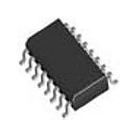
LTC1064-4CS Linear Technology, LTC1064-4CS Datasheet

LTC1064-4CS
Specifications of LTC1064-4CS
Available stocks
Related parts for LTC1064-4CS
LTC1064-4CS Summary of contents
Page 1
... Cauer response with lower noise and lower delay nonlinearity than the Cauer response. The stopband attenuation at 2.5 × f 50kHz can be achieved. The LTC1064-4 features low noise and low harmonic distortion even when input voltages applied. The LTC1064-4 overall performance competes with equivalent multiple op amp active realizations. The LTC1064-4 is pin compatible with the LTC1064-1, LTC1064-2 and LTC1064-3 ...
Page 2
... CUTOFF CUTOFF + – = ±2.37V = ±5V = ±7.5V = ±5V, Input = 1V at 1kHz RMS = ±7.5V, Input = 3V at 1kHz RMS = ±5V, Input = GND 1Hz to 999kHz = ±7.5V, Input = GND 1Hz to 999kHz ORDER PART NUMBER TOP VIEW R( LTC1064-4CSW COMP2 15 – CLK RATIO OUT SW PACKAGE = 150°C, θ ...
Page 3
... V = ±7. 25° 20kHz 1MHz, 50:1 CLK 90 135 180 225 270 315 360 405 450 FREQUENCY (kHz) LTC1064-4 = 1MHz 20kHz 10k, TTL clock input CLK C MIN TYP MAX ± 50 ±160 –100 –200 3/1 200 ±2.37 ±8 Passband Group Delay 220 V S 200 T = 25° ...
Page 4
... LTC1064 TYPICAL PERFOR A CE CHARACTERISTICS Gain vs Frequency with Compensation 125° 25°C A –5 –10 –15 – ±7. 5MHz –25 CLK RATIO = 50:1 –30 FOR COMPENSATION INFORMATION SEE PIN DESCRIPTION SECTION –35 10k 100k 1M FREQUENCY (Hz) 1064-4 G04 Power Supply Current vs Power Supply Voltage ...
Page 5
... LTC1064-4 PHASE (deg) –59.990 –122.400 169.300 88.500 –26.100 –175.100 126.500 87.600 38.400 –47.860 – , Typical Response = ±5V 25° 100kHz, Ratio = 100 CLK ...
Page 6
... LTC1064 TYPICAL PERFOR A CE CHARACTERISTICS Table 7. Gain/Phase for Figure 6. + Typical Response, Pin CUTOFF V = ±7.5V 2MHz, Ratio = 50:1 S CLK FREQUENCY (kHz) GAIN (dB) 10.000 –0.094 12.000 –0.100 14.000 –0.090 16.000 –0.080 18.000 –0.060 20.000 –0.040 22.000 –0.020 24.000 0.000 26.000 0.020 28.000 0.030 30 ...
Page 7
... Pin 10 should be tied For an f 100:1, Pin 10 should be tied to V midsupplies (i.e. ground), the filter response is neither Cauer nor transitional. Table 6 illustrates this response. Bypassing Pin 10 with a 0.1µF capacitor reduces the already small clock feedthrough. LTC1064-4 /f ratio of 50:1, CLK C /f ratio of CLK – ...
Page 8
... AGND 6 V COMP1* OUT 7 INV A 1064-4 F03 RECOMMENDED OP AMPS Clock LT1022, LT318, LT1056 Figure 4. Buffering the Filter Output. The Buffer Op Amp Should Not Share the LTC1064-4 Power Lines. 14 R(h, I) INV C 13 COMP2 – V LTC1064-4 12 – V AGND 0.1µF 11 ...
Page 9
... RAD TYP 0° – 15° .045 – .065 (1.143 – 1.651) .014 – .026 (0.360 – 0.660) OBSOLETE PACKAGE LTC1064 .220 – .310 (5.588 – 7.874 .200 (5.080) MAX .015 – .060 (0.381 – 1.524) .100 .125 (2.54) (3.175) ...
Page 10
... LTC1064-4 PACKAGE DESCRIPTIO .300 – .325 (7.620 – 8.255) .008 – .015 (0.203 – 0.381) +.035 .325 –.015 ( ) +0.889 8.255 –0.381 NOTE: INCHES 1. DIMENSIONS ARE MILLIMETERS *THESE DIMENSIONS DO NOT INCLUDE MOLD FLASH OR PROTRUSIONS. MOLD FLASH OR PROTRUSIONS SHALL NOT EXCEED .010 INCH (0.254mm) ...
Page 11
... NOTE 3 N/2 1 .093 – .104 × 45° (2.362 – 2.642) 0° – 8° TYP .050 (1.270) BSC .014 – .019 (0.356 – 0.482) LTC1064-4 .398 – .413 (10.109 – 10.490) NOTE .394 – .419 (10.007 – 10.643) N/2 ...
Page 12
... FAX: (408) 434-0507 –7.5V 0.1µF ≤2MHz 7. OUT Figure 7. Compensating LTC1064-4 for f Gain at f CUTOFF COMMENTS S0-8 Package, Low Power S0-8 Package, Very Low Power Internal Precision Clock, Low Power, S0-8 Package Internal Precision Clock, Delay Equalized, S0-8 Package www.linear.com 30pF 1M 1 ...


