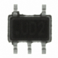
USBDF02W5 STMicroelectronics, USBDF02W5 Datasheet

USBDF02W5
Specifications of USBDF02W5
Available stocks
Related parts for USBDF02W5
USBDF02W5 Summary of contents
Page 1
... USBDF01W5 33 USBDF02W5 15 Tolerance ±10% Order codes Part number USBDF01W5 USBDF02W5 Benefits ■ EMI / RFI noise suppression ■ Required line termination for USB downstream ports ■ ESD protection exceeding IEC61000-4-2 level 4 ■ IPAD™ technology provides high flexibility in the design of high density boards ■ ...
Page 2
Characteristics 1 Characteristics Table 1. Absolute maximum ratings (T Symbol ESD discharge IEC 61000-4-2, contact discharge V PP ESD discharge - MIL STD 883 - Method 3015-6 T Operating junction temperature range j T Storage temperature range stg T Lead ...
Page 3
USBDFxxW5 Figure 2. Application example Host/Hub USB port transceiver 2.1 EMI filtering Current FCC regulations requires that class B computing devices meet specified maximum levels for both radiated and conducted EMI. ● Radiated EMI covers the frequency range from 30 ...
Page 4
Application information Figure 3. Measurement configuration 50 TG OUT Vg 2.2 ESD protection In addition to the requirements of termination and EMC compatibility, computing devices are required to be tested for ESD susceptibility. This test is described in the IEC ...
Page 5
USBDFxxW5 To have a good approximation of the remaining voltages at both V the typical dynamical resistance value R R > > R and input ...
Page 6
Application information Figure 7. Remaining voltage at both stages S1 (V surge Note that the USBDFxxW5 is not only acting for positive ESD surges but also for negative ones. Negative disturbances are clamped close to ground voltage as shown in ...
Page 7
USBDFxxW5 Figure 9. Analog crosstalk measurements TEST BOARD 50 TG OUT Vg Figure 8. gives the measurement circuit for the analog crosstalk application. In the curve shows the effect of the D+ cell on the D- cell. In usual frequency ...
Page 8
Application information 2.5 Transition times This low pass filter has been designed in order to meet the USB 1.1 standard requirements that implies the signal edges are maintained within the 4 ns-20 ns stipulated USB specification limits. Figure 13. Typical ...
Page 9
USBDFxxW5 3 Package information Table 3. SOT323-5L dimensions Figure 15. Recommended footprint (dimensions in mm) In order to meet environmental requirements, ST offers these devices in ECOPACK® packages. These packages have a lead-free second level ...
Page 10
... Ordering information 4 Ordering information Type USBDF01W5 USBDF01W5 USBDF02W5 USBDF02W5 5 Revision history Date May-2000 7-Sep-2006 15-Sep-2006 10/11 Order Code Weight 5.4 mg Revision 1C Initial release. Reformatted to current standard. Modified Operating junction 2 temperature range in Table 1. 3 Corrected units of R Marking Package UD1 SOT323-5L UD2 Changes to k instead of ...
Page 11
... USBDFxxW5 Information in this document is provided solely in connection with ST products. STMicroelectronics NV and its subsidiaries (“ST”) reserve the right to make changes, corrections, modifications or improvements, to this document, and the products and services described herein at any time, without notice. All ST products are sold pursuant to ST’s terms and conditions of sale. ...


