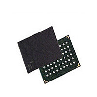
MT45W1MW16PDGA-70 IT Micron Technology Inc, MT45W1MW16PDGA-70 IT Datasheet - Page 12

MT45W1MW16PDGA-70 IT
Manufacturer Part Number
MT45W1MW16PDGA-70 IT
Description
Manufacturer
Micron Technology Inc
Datasheet
1.MT45W1MW16PDGA-70_IT.pdf
(29 pages)
Specifications of MT45W1MW16PDGA-70 IT
Operating Temperature (max)
85C
Operating Temperature (min)
-40C
Mounting
Surface Mount
Operating Temperature Classification
Industrial
Lead Free Status / RoHS Status
Compliant
Low-Power Operation
Standby Mode Operation
Temperature-Compensated Refresh
Partial-Array Refresh
PDF: 09005aef81cadc83/Source:09005aef81c6edb4
16mb_asyncpage_cr1_0_p23z_2.fm - Rev. F 4/08 EN
During standby, the device current consumption is reduced to the level necessary to per-
form the DRAM refresh operation on the full array. Standby operation occurs when CE#
and ZZ# are HIGH.
The device will enter a reduced power state during READ and WRITE operations where
the address and control inputs remain static for an extended period of time. This mode
will continue until a change occurs to the address or control inputs.
Temperature-compensated refresh (TCR) allows for adequate refresh at different tem-
peratures. This CellularRAM device includes an on-chip temperature sensor. When the
sensor is enabled, it continually adjusts the refresh rate according to the operating tem-
perature. The on-chip sensor is enabled by default.
Three fixed refresh rates are also available, corresponding to temperature thresholds of
+15°C, +45°C, and +85°C. The setting selected must be for a temperature higher than the
case temperature of the CellularRAM device. If the case temperature is +35°C, the system
can minimize self refresh current consumption by selecting the +45°C setting. Using the
+15°C setting in the same environment would result in an inadequate refresh rate and
cause data corruption.
Partial-array refresh (PAR) restricts refresh operation to a portion of the total memory
array. This feature enables the system to reduce refresh current by only refreshing that
part of the memory array that is absolutely necessary. The refresh options are full array,
one-half array, one-quarter array, one-eighth array, or none of the array. Data stored in
addresses not receiving refresh will become corrupted. The mapping of these partitions
can start at either the beginning or the end of the address map (Table 3 on page 17).
READ and WRITE operations are ignored during PAR operation.
The device only enters PAR mode if the SLEEP bit in the CR has been set HIGH
(CR[4] = 1). PAR can be initiated by bring the ZZ# ball to the LOW state for longer than
10µs. Returning ZZ# to HIGH will cause an exit from PAR and the entire array will be
immediately available for READ and WRITE operations.
Alternatively, PAR can be initiated using the CR software access sequence (see “Software
Access to the Configuration Register” on page 14). PAR is enabled immediately upon set-
ting CR[4] to “1” using this method. However, using software access to write to the CR
alters the function of ZZ# so that ZZ# LOW no longer initiates PAR, although ZZ# contin-
ues to enable WRITEs to the CR. This functional change persists until the next time the
device is powered up (see Figure 8).
16Mb: 1 Meg x 16 Async/Page CellularRAM 1.0 Memory
12
Micron Technology, Inc., reserves the right to change products or specifications without notice.
Low-Power Operation
©2005 Micron Technology, Inc. All rights reserved.


